SLVA478C October 2013 – November 2022 TPS62120 , TPS62122
3 Startup Behavior and Switching Node Consideration
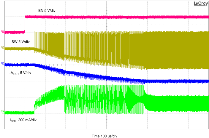
Figure 3-1 shows the startup behavior in the inverting configuration. After EN is taken high, the device starts switching after about a 50-µs delay. Due to the higher peak currents in the inverting topology, current limit is frequently reached during startup. This is acceptable as long as the saturation current of the inductor is chosen appropriately.
 Figure 3-1 Startup Behavior in the Inverting Configuration
Figure 3-1 also shows the SW node voltage as the device starts up. The voltage on the SW pin switches from VIN to VOUT. As the high-side MOSFET turns on, the SW node sees the input voltage and as the low-side MOSFET turns on, the SW node sees the IC ground, which is the output voltage. As VOUT continues to ramp down, the SW node low level follows it down.