SLVA478C October 2013 – November 2022 TPS62120 , TPS62122
1.3 Output Current Calculations
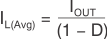
The average inductor current is affected in this topology. In the buck configuration, the average inductor current equals the average output current because the inductor always supplies current to the load during both the on and off times of the control MOSFET. However, in the inverting buck boost configuration, the load is supplied with current only from the output capacitor and is completely disconnected from the inductor during the on time of the control MOSFET. During the off time, the inductor connects to both the output cap and the load (see Figure 1-3). Knowing that the off time is 1 – D of the switching period, then the average inductor current is:
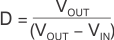
The duty cycle for the typical buck converter is simply VOUT / VIN but the duty cycle for an inverting buck boost converter becomes:
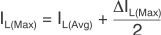
Finally, the maximum inductor current becomes:
Where,
D: Duty cycle
∆IL (A): Peak to peak inductor ripple current
VIN (V): Input voltage with respect to ground, instead of IC ground or –VOUT.
The TPS62120’s current limit technique allows a simple maximum output current calculation. If the current exceeds ILIMF (the high-side MOSFET current limit), the high-side MOSFET switch turns off and the low-side MOSFET switch turns on until the inductor current ramps down to 0. If an overload is still present after reaching 0 current, the low-side MOSFET switch turns off and the high-side MOSFET switch turns on until current limit is reached again. In current limit, the inductor’s current goes from ILIMF to 0—its ripple current becomes ILIMF. Operating the TPS62120 in this state (with IL(Max) equal to ∆IL(Max) equal to ILIMF) reduces the average inductor current to ½ ILIMF (from Equation 3). With the TPS62120's minimum current limit value of 200 mA, this gives an IL(Avg) of 100 mA when current limit is reached. With this, the maximum allowable output current is calculated from Equation 1 and Equation 2, with a 5-V input voltage to –5-V output voltage system as an example:
D = –5 / (–5 – 5) = 0.5
This result is then used in Equation 1:
IOUT = IL(Avg) × (1 – D) = 100 × (1 – 0.5) = 50 mA
The maximum output current for –5 V, –3.3 V and –1.8 V output voltages at different input voltages is displayed in Figure 1-4.
 Figure 1-4 Maximum Output Current versus Input Voltage