SLVA833D October 2016 – May 2021 TPS2660 , TPS2662 , TPS2663
- Trademarks
- 1 Surge Test (IEC 61000-4-5)
- 2 EFuse Solution for Surge Protection
- 3 EFuse Solution Schematic for Surge Protection
- 4 Circuit Performance for Surge Tests
- 5 EFT Test (IEC 61000-4-4)
- 6 EFuse Solution Schematic for EFT protection
- 7 Circuit Performance for EFT Tests
- 8 Power-Fail Test (IEC 61000-4-29)
- 9 EFuse Solution Schematic for Power-Fail Applications
- 10Circuit Performance for Power-Fail Tests
- 11EFT, Surge and Power-Fail Test Setup
- 12Conclusion
- 13References
- 14Revision History
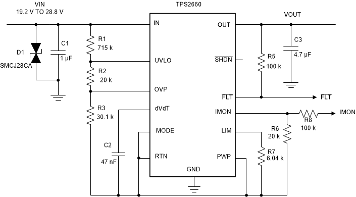
3 EFuse Solution Schematic for Surge Protection
 Figure 3-1 Efuse Solution Schematic for
Surge Protection
Figure 3-1 Efuse Solution Schematic for
Surge ProtectionThe complete schematic of the surge protection solution is shown in Figure 3-1. This protection circuit is designed for a 19.2 V to 28.8 V supply voltage range and 2-A load current. A 28-V reverse standoff voltage TVS in SMC package is used to clamp the surge voltage. When a ±500 V, 2Ω surge pulse is applied, the input voltage clamps to a ±44 V maximum. The Internal FET experiences maximum stress during the negative surge event. Maximum voltage across the device is the sum of the input clamp voltage and the output voltage under no load conditions. The maximum device stress at nominal test input voltage is less than the transient absolute maximum rating of the device with the selected TVS.