SLVAES9A June 2020 – July 2020 TPS1H000-Q1 , TPS1H100-Q1 , TPS1H200A-Q1 , TPS27S100 , TPS2H000-Q1 , TPS2H160-Q1 , TPS4H000-Q1 , TPS4H160-Q1
2.2 Inductive Loading and Loss of Battery
One concern when dealing with loss of battery faults is how to handle the negative voltage spike that is associated with driving an inductive load. During this turnoff, an unwanted voltage spike occurs on the output of the high-side switch due to the sudden turn off of the inductive load. In cases where a loss of battery condition is possible, having an inductive discharge clamp from VOUT to VS is not possible as the potential on VS will be undefined. Instead the designer has two options:
- Connecting a flyback diode in parallel with the load
- Use of a resistor/diode network on GND pin and serial protection resistors
The first option of connecting a flyback diode in parallel with the inductive load is a safe way of decoupling the voltage spike from the upstream high-side switch. In this approach the energy is dissipated across the circular path in parallel with the load as Figure 2-1 shows:
 Figure 2-1 Current Path for Flyback
Diode
Figure 2-1 Current Path for Flyback
DiodeAs the current path is dissipated across the diode, the negative voltage seen at the output of the high-side switch will be approximately equal to the negative forward voltage of the diode (typically –0.7 V). While this method has the advantage of decoupling the high-side switch completely from the inductive discharge process it is considerably slower versus dissipating the inductive load across the switch. Specifically, you can use the following current decay formula for flyback diode to model how long it would take for an inductive load to decay:
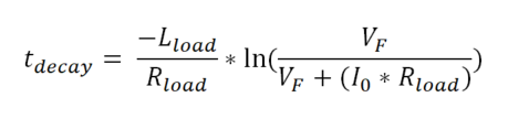
For example, suppose there was a 100-mH inductive load that had an initial current of 1 A and a series load resistance of 10 Ω. Also presume that the design is using a standard diode with a forward voltage drop of 0.7 V. Plugging this into the previous formula yields the example flyback current decay as follows:
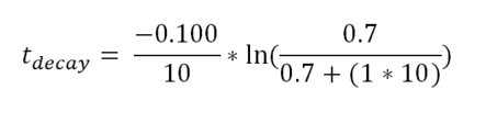
This calculates out to a total decay time of 27.3 ms. As a comparison, looking at the same loading conditions being discharged over the integrated VDS clamp of the TPS1H100, this would equate to a discharge time of approximately 1.76 ms with a 18-V supply rail and 70-V integrated VDS clamp (see the How To Drive Resistive, Inductive, Capacitive, and Lighting Loads With Smart High Side Switches Application Report for details on this calculation). One common mitigation to this problem is to replace the standard flyback diode with a Zener diode and regular diode in parallel with the load as Figure 2-2 shows:
 Figure 2-2 Zener Diode for Inductive
Loading
Figure 2-2 Zener Diode for Inductive
LoadingIn this scenario, the Zener diode allows the voltage spike being caused by the discharging inductor to be clamped at a higher voltage level versus the normal diode. This essentially leads to an output potential on the load of the negative Zener voltage of the Zener diode. The normal diode is placed in series with the Zener diode to prevent any forward biasing of the Zener diode. Using the same loading conditions as previously stated in Equation 2 and using a Zener voltage of something like 10 V, the following Zener calculation is attained:
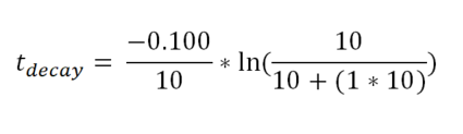
This leads to a total current decay time of the inductor of 6.9 ms. Increasing the Zener voltage of the diode results in a quicker discharge time; however, it also results in a high potential present on the output pin. Care must be taken to ensure downstream power components can handle the Zener voltage chosen.
It is also important to note that when a loss of battery condition occurs, a sudden and sharp decrease of the input voltage will be seen. If there is not sufficient capacitance on the input of the high-side switch, this can cause a fault condition where the negative voltage of the Zener clamp will be seen on the input of the switch itself. In this fault condition, the negative voltage on the supply pin will cause current to be drawn in through both the GND pin as well as the control and sense pins of the high-side switch. For TPSxHxx devices, if there is no diode on the GND pin of the high-side switch and there is sufficient current being injected into the GND pin, the parasitic latch on described in Section 1.3 might occur.
With a negative voltage on the input the ESD cells of the device can potentially break down and cause damage to the device. To mitigate the risk of this fault condition from happening the following design considerations are recommended:
- A diode on the GND pin of the high-side switch to block any negative current (follow the guidance in the device data sheet)
- A resistor on the GND pin of the high-side switch to pull the device ground to 0 V during a normal (no loss of battery) inductive turnoff
- Sufficient capacitance on the VS pin of the high-side switch to allow the internal FET to discharge and prevent the VS pin from going negative
- A unidirectional TVS diode from system ground to the VS pin to prevent the VS pin from going excessively negative (where possible)
Alternatively, if the flyback diode configuration is not possible due to size constraints or timing requirements it is possible to discharge small inductive load via the ground protection network on the TI high-side switch and serial protection resistors connected to the microcontroller. With this method the majority of the current is dissipated by both the protection resistors connected in series with the microcontroller pins and the ground resistor connected to the high-side switch. Figure 2-3 provides an illustration of this:
 Figure 2-3 Series Resistor
Protection
Figure 2-3 Series Resistor
ProtectionNote that this only works for very small inductances on the load that can mainly be attributed to cable lengths and parasitic values that typically equate to a few μH. In this setup, there are protections to prevent an overvoltage and this solution relies exclusively on the current-limiting capabilities of the protection/ground resistors as well as the robustness of the input/output pins of the high-side switch.