SLVAES9A June 2020 – July 2020 TPS1H000-Q1 , TPS1H100-Q1 , TPS1H200A-Q1 , TPS27S100 , TPS2H000-Q1 , TPS2H160-Q1 , TPS4H000-Q1 , TPS4H160-Q1
1.3 Output Protection on TPSxHxx Devices
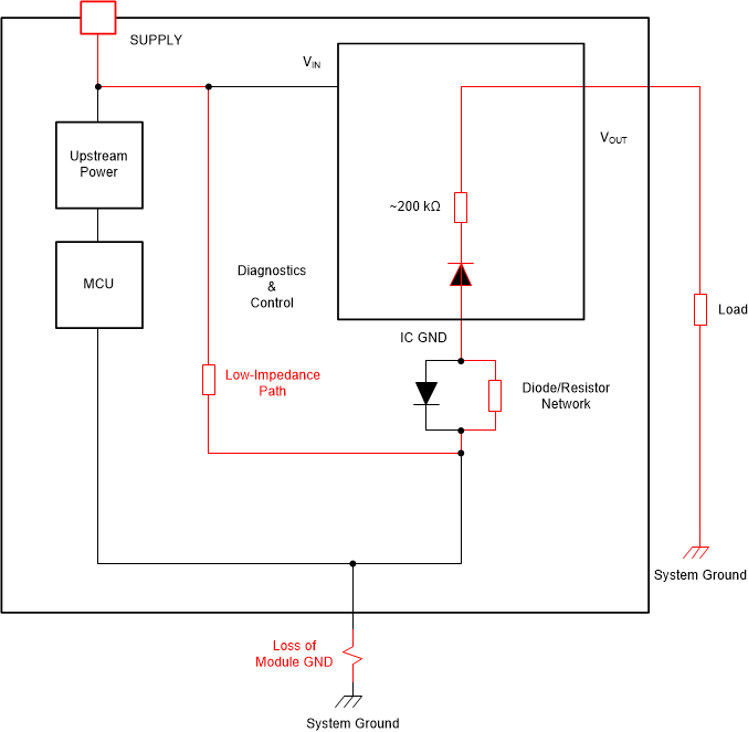
One corner case that needs to be considered on TPSxHxx smart high-side switch devices is a special condition where a loss of module ground occurs while there is a low-impedance path from the supply line to module ground. Figure 1-3 illustrates this condition.
 Figure 1-3 Low-Impedance Path
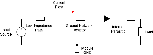
In the TPSxHxx device family there exists an approximately 200-kΩ internal parasitic path from the ground pin to the output pin of the switch itself. Without proper protection when a loss of device ground occurs a current path can exist through the TPSxHxx device. This current path starts from the supply voltage line, passes through the external low-impedance element, continues through the ground network resistor, continues through the internal parasitic path, and outputs to the attached load of the device. Figure 1-4 illustrates this current path.
 Figure 1-4 Parasitic Path
This parasitic current path can cause the internal FET of the TPSxHxx to partially and potentially fully bias and in effect output a voltage on the load regardless of whether the device is enabled or not. It is important to note that this fault condition will only occur when the following conditions hold true:
- A low-impedance path exists between the input supply line and the module ground of the high-side switch
- A module loss of ground exists as described in Section 1.2
It is also important to note that this phenomenon is only observed on the TPSxHxx device family. In the newer generation high-side switches, such as the TPSxHBxx or TPSxHAxx devices, this 200-kΩ parasitic path between the device ground pin and output does not exist and this fault condition is non-existent. Table 1-1 lists the devices affected by this issue.
| Device |
|---|
| TPS1H000-Q1 |
| TPS2H000-Q1 |
| TPS1H200-Q1 |
| TPS1H100-Q1 |
| TPS2H160-Q1 |
| TPS27S100 |
| TPS4H000-Q1 |
| TPS4H160-Q1 |
Note that in every device listed in Table 1-1, all versions of the specified device are affected. For example. for the TPS1H100-Q1 device, both the TPS1H100A-Q1 and TPS1H100B-Q1 are affected.
A key metric here is what is considered a “low” enough impedance between supply input and module ground to cause this fault. This fault will occur when the voltage at the ground pin is within approximately 500 mV to 1 V of the supply line voltage. Figure 1-5 illustrates the equivalent circuit and current path.
 Figure 1-5 Equivalent Current Path
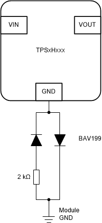
To protect against this double fault condition, appropriate design considerations have to be made to the resistor/diode network connected between the ground pin of the high-side switch and the local device ground. The data sheet of each device may vary; however, the general recommendation is to place a 1-kΩ resistor in parallel with a diode that has a forward current greater than 100 mA. To protect against the described about parasitic fault condition, it is recommended to increase the value of the resistor on the ground network to around 2 kΩ and to change the unidirectional diode to steering diode configuration such as the BAV199. Figure 1-6 illustrates this solution.
 Figure 1-6 Solution