SLVAEX7A December 2020 – January 2023 OPA2310 , OPA310 , OPA348 , OPA4310 , TLV341 , TLV341A , TLV342 , TLV342A
2.1 Standard Op Amp ESD Protection: Structure
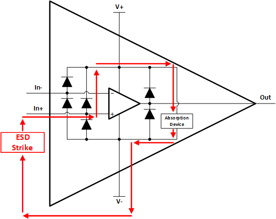
The majority of op amps have input structures that include a protection diode between each input and each supply rail, as shown in Figure 2-1. The purpose of these diodes is to protect the amplifier from sudden ESD strikes by clamping the rising voltage and redirecting the current surge away from the input stage transistors. If either input reaches a voltage greater than V+ plus the forward voltage of the ESD protection diode, the protection diodes become forward biased and the current flows from the input, through the ESD cell. In a similar manner, if either input reaches a voltage lower than V– minus the forward voltage of the ESD protection diode, the protection diodes become forward biased and the current flows through the ESD cell, to the input. Note that the forward voltage drop of the ESD diode is about 500 mV in many data sheets.
During an ESD event, several current paths are available, including through the absorption device, and the path taken depends on the voltages at the pins. An example is shown in Figure 2-1 where the IN+ pin takes a large, positive voltage with respect to V–.
 Figure 2-1 Path of Current During ESD Strike From In+ to V– for Op Amp With Standard ESD Protection
The behavior of the output protection diodes, also seen in Figure 2-1, mirrors that of the input protection diodes. If the output reaches a voltage higher than V+ plus the forward voltage of the ESD diode, a current path forms and current flows from the output, through the ESD cell. The same occurs if the output reaches a voltage lower than V– minus the forward voltage of the ESD diode, a current path forms and current flows through the ESD cell, to the output.
Note that ESD protection is for out-of-circuit events, such as ESD events that can occur during handling or assembly, and is not intended for in-circuit events. Because this protection structure is designed for high-energy, short-duration ESD events, the diodes must be protected from destruction during the longer instances of Electrical Overstress (EOS). During EOS events, the applied voltage can be a lot lower. For example, the voltage can be in the region of 500 mV over the supply voltage rather than 1 kV. However, these scenarios also last for much longer periods of time. The level of current that the protection diodes can sustain under EOS is often given in the Absolute Maximum Ratings section of the data sheet as ±10 mA. Nonetheless, keep this number under ±1 mA, when possible.
If the circuit designer anticipates the possibility of either input going outside the minimum or maximum common-mode voltage range in the Absolute Maximum Ratings table of the data sheet, a common practice is to include series resistors at the IN+ and IN– pins that are sized to limit the input current. Additional ESD and EOS scenarios are covered in more depth in the TI Precision Labs presentations on ESD and EOS.
Table 2-1 shows an example Absolute Maximum Ratings table from the TLV9051 / TLV9052 / TLV9054 5-MHz, 15-V/μs High Slew-Rate, RRIO Op Amp data sheet. Limit the common-mode voltage to be no less than (V–) – 0.5 V and no more than (V+) + 0.5 V. If these limits are exceeded, the diode starts conducting current. If the current is high enough, the current can potentially damage the diodes themselves and cause subsequent damage to the amplifier inputs.
| MIN | MAX | UNIT | |||
|---|---|---|---|---|---|
| Supply voltage, VS = (V+) – (V–) | 7 | V | |||
| Signal input pins | Voltage(1) | Common-mode | (V–) – 0.5 | (V+) + 0.5 | V |
| Differential | VS + 0.2 | V | |||
| Current(1) | –10 | 10 | mA | ||
| Output short-circuit(2) | Continuous | ||||
| Operating ambient temperature, TA | –40 | 150 | °C | ||
| Junction temperature, TJ | 150 | °C | |||
| Storage temperature, Tstg | –65 | 150 | °C | ||