SLVAEX7A December 2020 – January 2023 OPA2310 , OPA310 , OPA348 , OPA4310 , TLV341 , TLV341A , TLV342 , TLV342A
3.1 Op Amp ESD Protection Without Input Diodes to V+: Structure
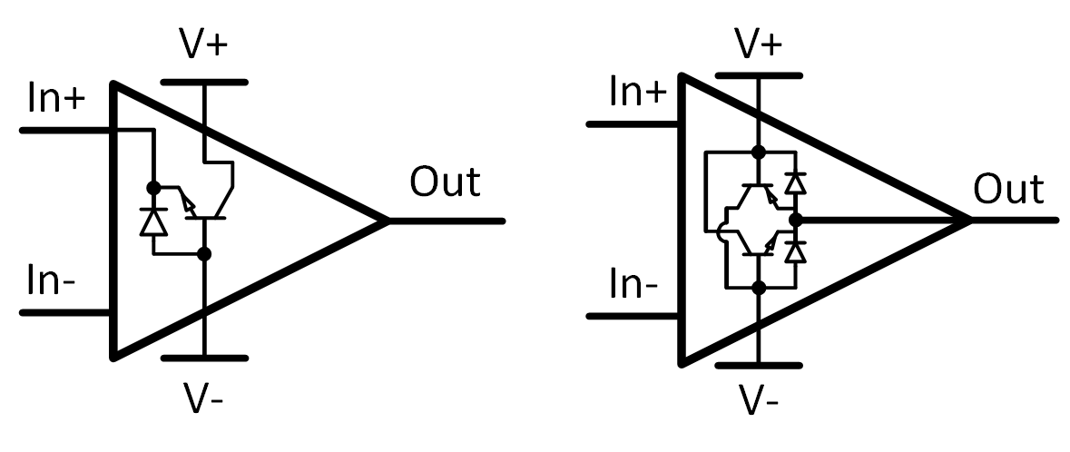
Figure 3-1 shows an example of an alternate input protection structure for the IN+ and OUT pins. The same structure is present on the IN– pin as on the IN+ pin, though the structure is not shown here for the sake of simplicity. In contrast, the output pin has diode paths to both rails. Not all of the input protection is shown here, instead, this figure shows only the portion most relevant to this application report.
 Figure 3-1 Current Paths for IN+ (also present for IN–) and OUT
Table 3-1 shows an example Absolute Maximum Ratings table from the OPAx310 High Output Current, Fast Shutdown, Low Voltage (1.5 V to 5.5 V), RRIO, 3-MHz Operational Amplifier. Unlike what was seen with a standard ESD protection structure table, where the absolute input common-mode voltages can only go 0.5 V past the supply rails, the input common-mode voltages of this alternative protection scheme do not have that limitation. There still is a limit to how far the input voltage can be taken beyond V+. Eventually, the input is driven too far and significant current begins to flow. Example test setups and sample data are provided later in this document.
| MIN | MAX | UNIT | ||
|---|---|---|---|---|
| Supply voltage, VS = (V+) – (V–) | 0 | 7 | V | |
| Signal input pins | Common-mode | – 0.5 | 6.0 | V |
| Differential | ±6.0 | V | ||
| Current(2) | –10 | 10 | mA | |
| Output short-circuit(3) | Continuous | |||
| Operating ambient temperature, TA | –55 | 150 | °C | |
| Junction temperature, TJ | 150 | °C | ||
| Storage temperature, Tstg | –65 | 150 | °C | |
Finally, remember that the devices with this alternative ESD protection structure still start to turn on their diode protection paths if one of the input pins falls below V– minus 0.5 V. Therefore, consider what type of input signals are present while the amplifier is turned off.