SLVAF01 October 2020 TPS55340
2.1 Zener or TVS Clamping
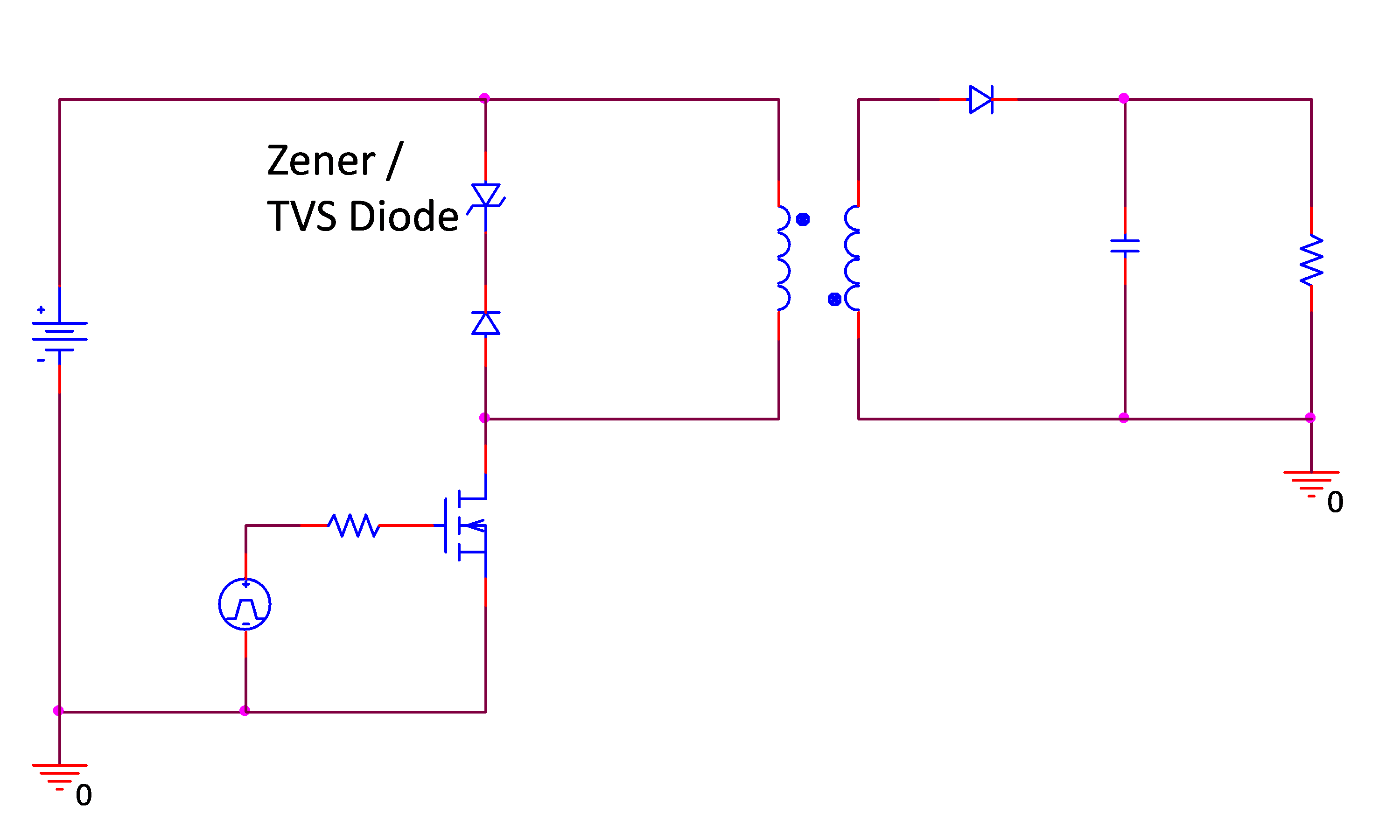
There are several ways to contain voltage spike by adding some snubber circuits but Zener / TVS clamping is strong candidate for the solution if the peak level should be limited so as to protect the switching device. This means that user easily controls peak level of voltage spike that is caused by leakage inductance from transformer by selecting proper zener diode’s Vz rating. Figure 2-1 is the simulation results about how the voltage spike could be mitigated according to zener voltage rating under a same leakage inductance, VOR and VIN condition. It shows how voltage shape on SW node is being changed. From left, Zener rating is 1.5 times of VOR, 1.3 times and 1.1 times of VOR. (VOR is 10 V, VIN is 18 V) Noticeably, voltage peak and ringing is being mitigated if Zener rating is getting close to VOR value.

 Figure 2-1 Voltage Spike on Switching
Node with Zener Rating
Figure 2-1 Voltage Spike on Switching
Node with Zener RatingThe main purpose of zener clamping is to absorb energy from leakage inductance when main switch is turned off, but it also could clamp some of energy from magnetizing inductance of primary winding if zener rating is very close to VOR level. It means some of the stored energy in the primary which is supposed to be delivered to secondary load during turn-off period may disappear in the zener block as Figure 2-2. So this should be optimized in the system, considering required voltage stress versus system efficiency.
 Figure 2-2 Secondary Current Shape
According to Zener Rating