SLVAF95 april   2023 TPS7H5001-SP


  1.   Abstract
  2.   Trademarks
  3.   Description
  4.   Features
  5.   Applications
  6. 1System Overview
    1. 1.1 Block Diagram
    2. 1.2 Design Considerations
    3. 1.3 System Design Theory
      1. 1.3.1 Switching Frequency
      2. 1.3.2 Transformer
      3. 1.3.3 RCD and Diode Clamp
      4. 1.3.4 Output Diode and MOSFET
      5. 1.3.5 Output Filter and Capacitance
      6. 1.3.6 Compensation
      7. 1.3.7 Controller Passives
  7. 2Test Results
    1. 2.1 Testing and Results
      1. 2.1.1 Test Setup
      2. 2.1.2 Test Results
        1. 2.1.2.1 Efficiency
        2. 2.1.2.2 Frequency Response
        3. 2.1.2.3 Thermal Characteristics
        4. 2.1.2.4 Output Voltage Ripple
        5. 2.1.2.5 Load Step
        6. 2.1.2.6 Start-Up
        7. 2.1.2.7 Shutdown
        8. 2.1.2.8 Component Stresses
  8. 3Design Files
    1. 3.1 Schematics
    2. 3.2 Bill of Materials
    3. 3.3 Assembly Drawings
  9. 4Related Documentation

Frequency Response

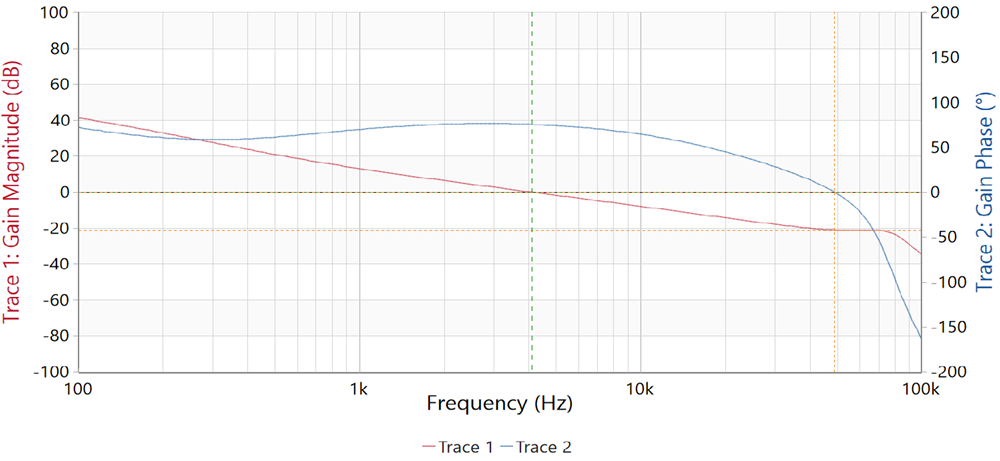
GUID-20230406-SS0I-WB3D-RVLJ-J2CPQBCVDTNZ-low.png Figure 2-2 28-VIN Frequency Response

Frequency response was taken with 10-A output current.

Table 2-2 Frequency Response Characteristics
PARAMETER VALUE
Crossover Frequency 4.12 kHz
Phase Margin 75.4°
Phase Crossover 49.1 kHz
Gain Margin –21.0 dB