SLVAF95 april   2023 TPS7H5001-SP


  1.   Abstract
  2.   Trademarks
  3.   Description
  4.   Features
  5.   Applications
  6. 1System Overview
    1. 1.1 Block Diagram
    2. 1.2 Design Considerations
    3. 1.3 System Design Theory
      1. 1.3.1 Switching Frequency
      2. 1.3.2 Transformer
      3. 1.3.3 RCD and Diode Clamp
      4. 1.3.4 Output Diode and MOSFET
      5. 1.3.5 Output Filter and Capacitance
      6. 1.3.6 Compensation
      7. 1.3.7 Controller Passives
  7. 2Test Results
    1. 2.1 Testing and Results
      1. 2.1.1 Test Setup
      2. 2.1.2 Test Results
        1. 2.1.2.1 Efficiency
        2. 2.1.2.2 Frequency Response
        3. 2.1.2.3 Thermal Characteristics
        4. 2.1.2.4 Output Voltage Ripple
        5. 2.1.2.5 Load Step
        6. 2.1.2.6 Start-Up
        7. 2.1.2.7 Shutdown
        8. 2.1.2.8 Component Stresses
  8. 3Design Files
    1. 3.1 Schematics
    2. 3.2 Bill of Materials
    3. 3.3 Assembly Drawings
  9. 4Related Documentation

Component Stresses

For the test in Figure 2-11 and Figure 2-12, 28 V was applied to the input and 10 A was drawn from the output. For the output FET and diode stress, the voltage was measured with respect to ground so the output voltage must be added to show the true stress on the output diode.
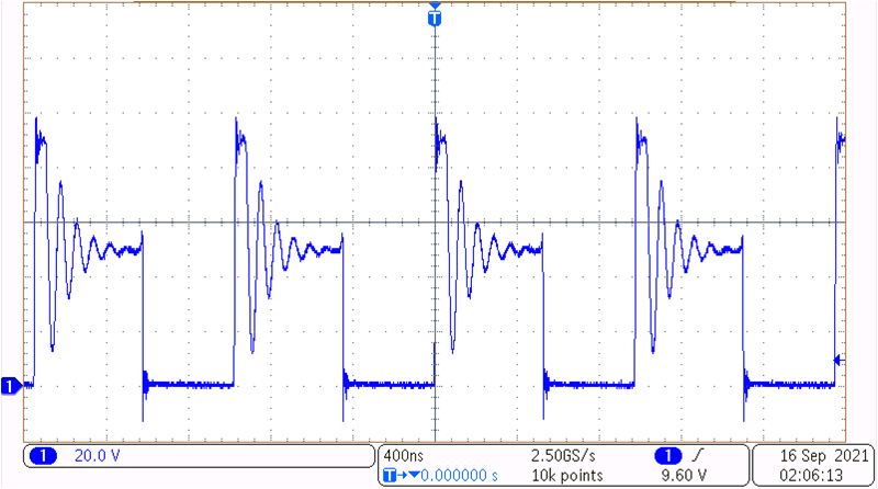
GUID-20230405-SS0I-7S2P-PNQX-DR2RN3XPC0M0-low.png Figure 2-11 Voltage Stress on Main Switching MOSFET
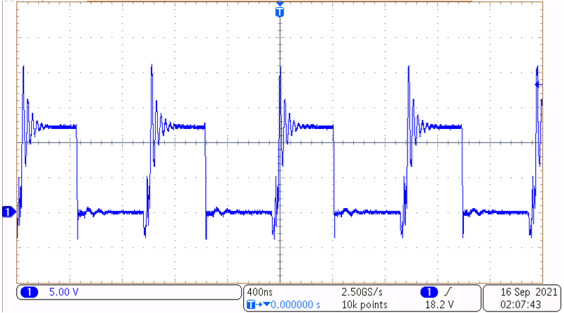
GUID-20230405-SS0I-59LJ-N23H-HFGMT3HZRZD3-low.png Figure 2-12 Output FET and Diode Stress