SLVAFI8 February 2023 TLC6C5748-Q1
- Abstract
- Trademarks
- 1Introduction
-
2Design Considerations for Low EMI
- 2.1 Design Considerations Overview
- 2.2
Considerations in Detail
- 2.2.1 Top-Level Architecture
- 2.2.2
High Frequency Signals
- 2.2.2.1 Original Setup
- 2.2.2.2 3.3 V I/O Voltage Instead of 5 V
- 2.2.2.3 Use Independent OSC for GSCLK With Spread Spectrum
- 2.2.2.4 Without Using Buffer on GSCLK
- 2.2.2.5 Using Snubber on GSCLK
- 2.2.2.6 Lower the Signal Frequency
- 2.2.2.7 Placement and PCB layout
- 2.2.2.8 ESD Enhancement
- 2.2.2.9 Demo and Test Results
- 2.2.2.10 Bench Test Results
- 3Summary
- 4References
2.2.2.3 Use Independent OSC for GSCLK With Spread Spectrum
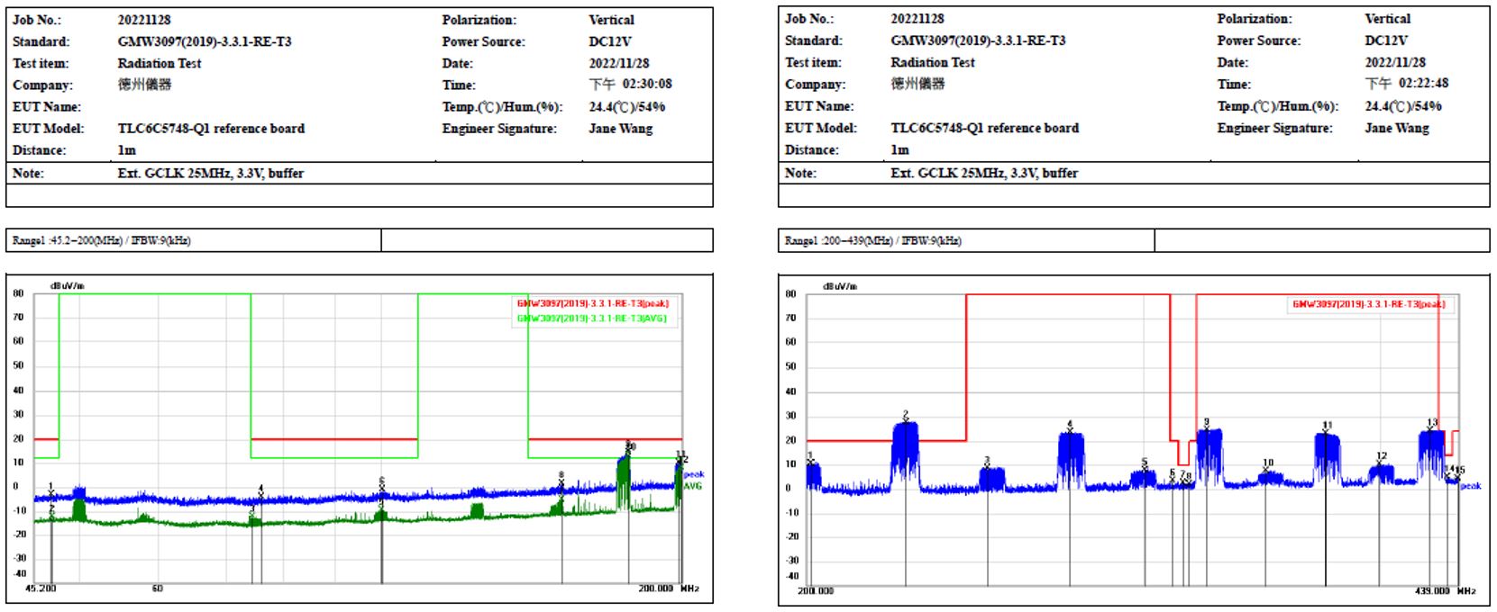
GUID-1523EE61-7DB1-4058-BEB8-19973910F6C7.html#FIG_TW3_BKL_FWB shows the high EMI noise peak generating from GSCLK. To avoid EMI noise peak, using spectrum independent OSC is the common method. Generally, micro-controller can generate the spread spectrum clock signal, but comparing with oscillator, it has high EMI noise commonly. Using The independent OSC can be placed nearest close to the first LED driver which means lower shorter signal path. #FIG_CQX_MKL_FWB shows test results using independent OSC for GSCLK with spread spectrum.
 Figure 2-5 Test Results of Using 3.3 V IO
Voltage Setup, GSCLK with SSC and Remove Buffer (Vertical Direction) from 45 MHz
to 439 MHz