SLVSCM2D October 2014 – December 2019 TPS1H100-Q1
PRODUCTION DATA.
- 1 Features
- 2 Applications
- 3 Description
- 4 Revision History
- 5 Pin Configuration and Functions
- 6 Specifications
-
7 Detailed Description
- 7.1 Overview
- 7.2 Functional Block Diagram
- 7.3
Feature Description
- 7.3.1 Accurate Current Sense
- 7.3.2 Programmable Current Limit
- 7.3.3 Inductive-Load Switching-Off Clamp
- 7.3.4
Full Protections and Diagnostics
- 7.3.4.1 Short-to-GND and Overload Detection
- 7.3.4.2 Open-Load Detection
- 7.3.4.3 Short-to-Battery Detection
- 7.3.4.4 Reverse-Polarity Detection
- 7.3.4.5 Thermal Protection Behavior
- 7.3.4.6 UVLO Protection
- 7.3.4.7 Loss of GND Protection
- 7.3.4.8 Loss of Power Supply Protection
- 7.3.4.9 Reverse Current Protection
- 7.3.4.10 Protection for MCU I/Os
- 7.3.5 Diagnostic Enable Function
- 7.4 Device Functional Modes
- 8 Application and Implementation
- 9 Power Supply Recommendations
- 10Layout
- 11Device and Documentation Support
- 12Mechanical, Packaging, and Orderable Information
7.3.4.10 Protection for MCU I/Os
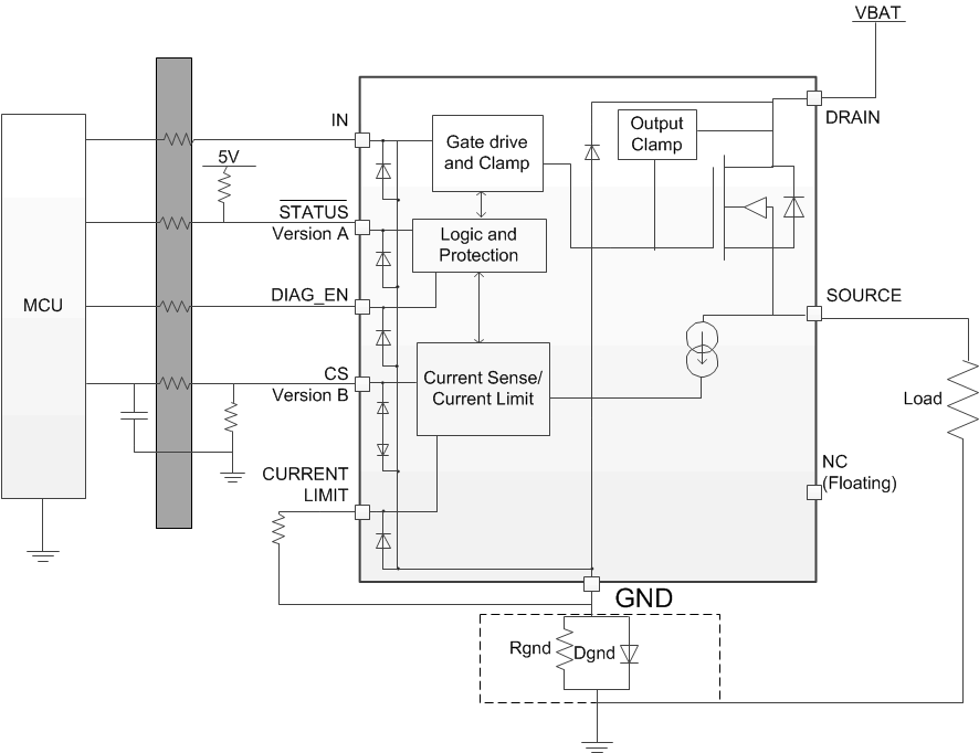
In many conditions, such as the negative ISO pulse, or the loss of battery with an inductive load, a negative potential on the device GND pin may damage the MCU I/O pins [more likely, the internal circuitry connected to the pins]. Therefore, the serial resistors between MCU and HSD are required.
Also, for proper protection against loss of GND, TI recommends 4.7 kΩ when using 3.3-V MCU I/Os; 10 kΩ is for 5-V applications.
 Figure 43. MCU IO Protections