SLVSCM2D October 2014 – December 2019 TPS1H100-Q1
PRODUCTION DATA.
- 1 Features
- 2 Applications
- 3 Description
- 4 Revision History
- 5 Pin Configuration and Functions
- 6 Specifications
-
7 Detailed Description
- 7.1 Overview
- 7.2 Functional Block Diagram
- 7.3
Feature Description
- 7.3.1 Accurate Current Sense
- 7.3.2 Programmable Current Limit
- 7.3.3 Inductive-Load Switching-Off Clamp
- 7.3.4
Full Protections and Diagnostics
- 7.3.4.1 Short-to-GND and Overload Detection
- 7.3.4.2 Open-Load Detection
- 7.3.4.3 Short-to-Battery Detection
- 7.3.4.4 Reverse-Polarity Detection
- 7.3.4.5 Thermal Protection Behavior
- 7.3.4.6 UVLO Protection
- 7.3.4.7 Loss of GND Protection
- 7.3.4.8 Loss of Power Supply Protection
- 7.3.4.9 Reverse Current Protection
- 7.3.4.10 Protection for MCU I/Os
- 7.3.5 Diagnostic Enable Function
- 7.4 Device Functional Modes
- 8 Application and Implementation
- 9 Power Supply Recommendations
- 10Layout
- 11Device and Documentation Support
- 12Mechanical, Packaging, and Orderable Information
7.3.4.5 Thermal Protection Behavior
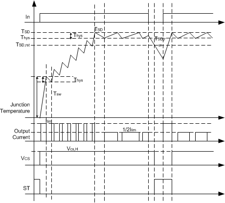
Both the absolute temperature thermal shutdown and the dynamic temperature thermal swing diagnostic and protection are built into the device to increase the maximum reliability of the power FET. Thermal swing is active when the temperature of the power FET is increasing sharply, that is ΔT = TDMOS – TLogic > Tsw, then the output is shut down, and the ST pin goes low, or the CS pin is pulled up to VCS,h. It auto-recovers and clears the fault signal until ΔT = TDMOS – TLogic < Tsw – Thys. Thermal swing function improves device reliability against repetitive fast thermal variation, as shown in Figure 37. Multiple thermal swings are triggered before thermal shutdown happens. Thermal shutdown is active when absolute temperature T > TSD. When active, the output is shut down, and the ST pin goes low, or the CS pin is pulled up to VCS,h. The output is auto-recovered when T < TSD – Thys; the current limit is reduced to Ilim,tsd, or half of the programmable current limit value, to avoid repeated thermal shutdown. However, the thermal shutdown fault signal and half-current limit value are not cleared until the junction temperature decreases to less than TSD,rst.
 Figure 37. Thermal Behavior