SLVSDR2B November   2018  – March 2021 ADC12DJ3200QML-SP

PRODUCTION DATA  

  1. Features
  2. Applications
  3. Description
  4. Revision History
  5. Pin Configuration and Functions
  6. Specifications
    1. 6.1  Absolute Maximum Ratings
    2. 6.2  ESD Ratings
    3. 6.3  Recommended Operating Conditions
    4. 6.4  Thermal Information
    5. 6.5  Electrical Characteristics: DC Specifications
    6. 6.6  Electrical Characteristics: Power Consumption
    7. 6.7  Electrical Characteristics: AC Specifications (Dual-Channel Mode)
    8. 6.8  Electrical Characteristics: AC Specifications (Single-Channel Mode)
    9. 6.9  Timing Requirements
    10. 6.10 Switching Characteristics
    11. 6.11 Timing Diagrams
    12. 6.12 Typical Characteristics
  7. Detailed Description
    1. 7.1 Overview
    2. 7.2 Functional Block Diagram
    3. 7.3 Feature Description
      1. 7.3.1 Analog Inputs
        1. 7.3.1.1 Analog Input Protection
        2. 7.3.1.2 Full-Scale Voltage (VFS) Adjustment
        3. 7.3.1.3 Analog Input Offset Adjust
      2. 7.3.2 ADC Core
        1. 7.3.2.1 ADC Theory of Operation
        2. 7.3.2.2 ADC Core Calibration
        3. 7.3.2.3 ADC Overrange Detection
        4. 7.3.2.4 Code Error Rate (CER)
      3. 7.3.3 Timestamp
      4. 7.3.4 Clocking
        1. 7.3.4.1 Noiseless Aperture Delay Adjustment (tAD Adjust)
        2. 7.3.4.2 Aperture Delay Ramp Control (TAD_RAMP)
        3. 7.3.4.3 SYSREF Capture for Multi-Device Synchronization and Deterministic Latency
          1. 7.3.4.3.1 SYSREF Position Detector and Sampling Position Selection (SYSREF Windowing)
          2. 7.3.4.3.2 Automatic SYSREF Calibration
      5. 7.3.5 Digital Down Converters (Dual-Channel Mode Only)
        1. 7.3.5.1 Numerically-Controlled Oscillator and Complex Mixer
          1. 7.3.5.1.1 NCO Fast Frequency Hopping (FFH)
          2. 7.3.5.1.2 NCO Selection
          3. 7.3.5.1.3 Basic NCO Frequency Setting Mode
          4. 7.3.5.1.4 Rational NCO Frequency Setting Mode
          5. 7.3.5.1.5 NCO Phase Offset Setting
          6. 7.3.5.1.6 NCO Phase Synchronization
        2. 7.3.5.2 Decimation Filters
        3. 7.3.5.3 Output Data Format
        4. 7.3.5.4 Decimation Settings
          1. 7.3.5.4.1 Decimation Factor
          2. 7.3.5.4.2 DDC Gain Boost
      6. 7.3.6 JESD204B Interface
        1. 7.3.6.1 Transport Layer
        2. 7.3.6.2 Scrambler
        3. 7.3.6.3 Link Layer
          1. 7.3.6.3.1 Code Group Synchronization (CGS)
          2. 7.3.6.3.2 Initial Lane Alignment Sequence (ILAS)
          3. 7.3.6.3.3 8b, 10b Encoding
          4. 7.3.6.3.4 Frame and Multiframe Monitoring
        4. 7.3.6.4 Physical Layer
          1. 7.3.6.4.1 SerDes Pre-Emphasis
        5. 7.3.6.5 JESD204B Enable
        6. 7.3.6.6 Multi-Device Synchronization and Deterministic Latency
        7. 7.3.6.7 Operation in Subclass 0 Systems
      7. 7.3.7 Alarm Monitoring
        1. 7.3.7.1 NCO Upset Detection
        2. 7.3.7.2 Clock Upset Detection
      8. 7.3.8 Temperature Monitoring Diode
      9. 7.3.9 Analog Reference Voltage
    4. 7.4 Device Functional Modes
      1. 7.4.1 Dual-Channel Mode
      2. 7.4.2 Single-Channel Mode (DES Mode)
      3. 7.4.3 JESD204B Modes
        1. 7.4.3.1 JESD204B Output Data Formats
        2. 7.4.3.2 Dual DDC and Redundant Data Mode
      4. 7.4.4 Power-Down Modes
      5. 7.4.5 Test Modes
        1. 7.4.5.1 Serializer Test-Mode Details
        2. 7.4.5.2 PRBS Test Modes
        3. 7.4.5.3 Ramp Test Mode
        4. 7.4.5.4 Short and Long Transport Test Mode
          1. 7.4.5.4.1 Short Transport Test Pattern
          2. 7.4.5.4.2 Long Transport Test Pattern
        5. 7.4.5.5 D21.5 Test Mode
        6. 7.4.5.6 K28.5 Test Mode
        7. 7.4.5.7 Repeated ILA Test Mode
        8. 7.4.5.8 Modified RPAT Test Mode
      6. 7.4.6 Calibration Modes and Trimming
        1. 7.4.6.1 Foreground Calibration Mode
        2. 7.4.6.2 Background Calibration Mode
        3. 7.4.6.3 Low-Power Background Calibration (LPBG) Mode
      7. 7.4.7 Offset Calibration
      8. 7.4.8 Trimming
      9. 7.4.9 Offset Filtering
    5. 7.5 Programming
      1. 7.5.1 Using the Serial Interface
        1. 7.5.1.1 SCS
        2. 7.5.1.2 SCLK
        3. 7.5.1.3 SDI
        4. 7.5.1.4 SDO
        5. 7.5.1.5 Streaming Mode
    6. 7.6 Register Maps
      1. 7.6.1 Register Descriptions
      2. 7.6.2 SYSREF Calibration Registers (0x2B0 to 0x2BF)
      3. 7.6.3 Alarm Registers (0x2C0 to 0x2C2)
  8. Application Information Disclaimer
    1. 8.1 Application Information
      1. 8.1.1 Analog Inputs
      2. 8.1.2 Analog Input Bandwidth
      3. 8.1.3 Clocking
      4. 8.1.4 Radiation Environment Recommendations
        1. 8.1.4.1 Single Event Latch-Up (SEL)
        2. 8.1.4.2 Single Event Functional Interrupt (SEFI)
        3. 8.1.4.3 Single Event Upset (SEU)
    2. 8.2 Typical Application
      1. 8.2.1 Design Requirements
      2. 8.2.2 Detailed Design Procedure
        1. 8.2.2.1 RF Input Signal Path
        2. 8.2.2.2 Calculating Values of AC-Coupling Capacitors
      3. 8.2.3 Application Curves
    3. 8.3 Initialization Set Up
  9. Layout
    1. 9.1 Layout Guidelines
    2. 9.2 Layout Example
  10. 10Device and Documentation Support
    1. 10.1 Device Support
      1. 10.1.1 Development Support
    2. 10.2 Documentation Support
      1. 10.2.1 Related Documentation
    3. 10.3 Receiving Notification of Documentation Updates
    4. 10.4 Community Resources
    5. 10.5 Trademarks

ADC Theory of Operation

The differential voltages at the analog inputs are captured by the rising edge of CLK± in dual-channel mode or by the rising and falling edges of CLK± in single-channel mode. After capturing the input signal, the ADC converts the analog voltage to a digital value by comparing the voltage to the internal reference voltage. If the voltage on INA– or INB– is higher than the voltage on INA+ or INB+, respectively, then the digital output is a negative 2's complement value. If the voltage on INA+ or INB+ is higher than the voltage on INA– or INB–, respectively, then the digital output is a positive 2's complement value. Equation 1 can calculate the differential voltage at the input pins from the digital output.
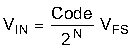
Equation 1. GUID-0ED6559A-65B2-4B8C-8D41-658D80495F17-low.gif

where

  • Code is the signed decimation output code (for example, –2048 to +2047)
  • N is the ADC resolution
  • and VFS is the full-scale input voltage of the ADC as specified in the Section 6.3 table, including any adjustment performed by programming FS_RANGE_A or FS_RANGE_B