SLVU411A September   2010  – June 2021 TPS62120


  1.   Trademarks
  2. 1Introduction
    1. 1.1 Features
    2. 1.2 Applications
  3. 2TPS62120EVM Schematic
  4. 3Connector and Test Point Descriptions
    1. 3.1 Enable Jumpers/Switches (RefDes) TPS62120
      1. 3.1.1  J1 VIN
      2. 3.1.2  J2 S+/S–
      3. 3.1.3  J3 GND
      4. 3.1.4  J4 VOUT
      5. 3.1.5  J5 S+/S–
      6. 3.1.6  J6 GND
      7. 3.1.7  JP1 EN
      8. 3.1.8  JP2 SGND
      9. 3.1.9  J7 VOUT (SMA)
      10. 3.1.10 J8 PG/GND
  5. 4Test Configuration
    1. 4.1 Hardware Setup
    2. 4.2 Procedure
  6. 5TPS62120EVM Test Data
    1. 5.1 Efficiency
    2. 5.2 Start-Up
    3. 5.3 Load Transient Response
    4. 5.4 Typical Operation, 60 mA
    5. 5.5 Typical Operation, 10 mA
    6. 5.6 Current Limit Operation
  7. 6TPS62120EVM Assembly Drawings and Layout
  8. 7Bill of Materials
  9. 8Revision History

Load Transient Response

Figure 5-6 illustrates the load transient response for the TPS62120.
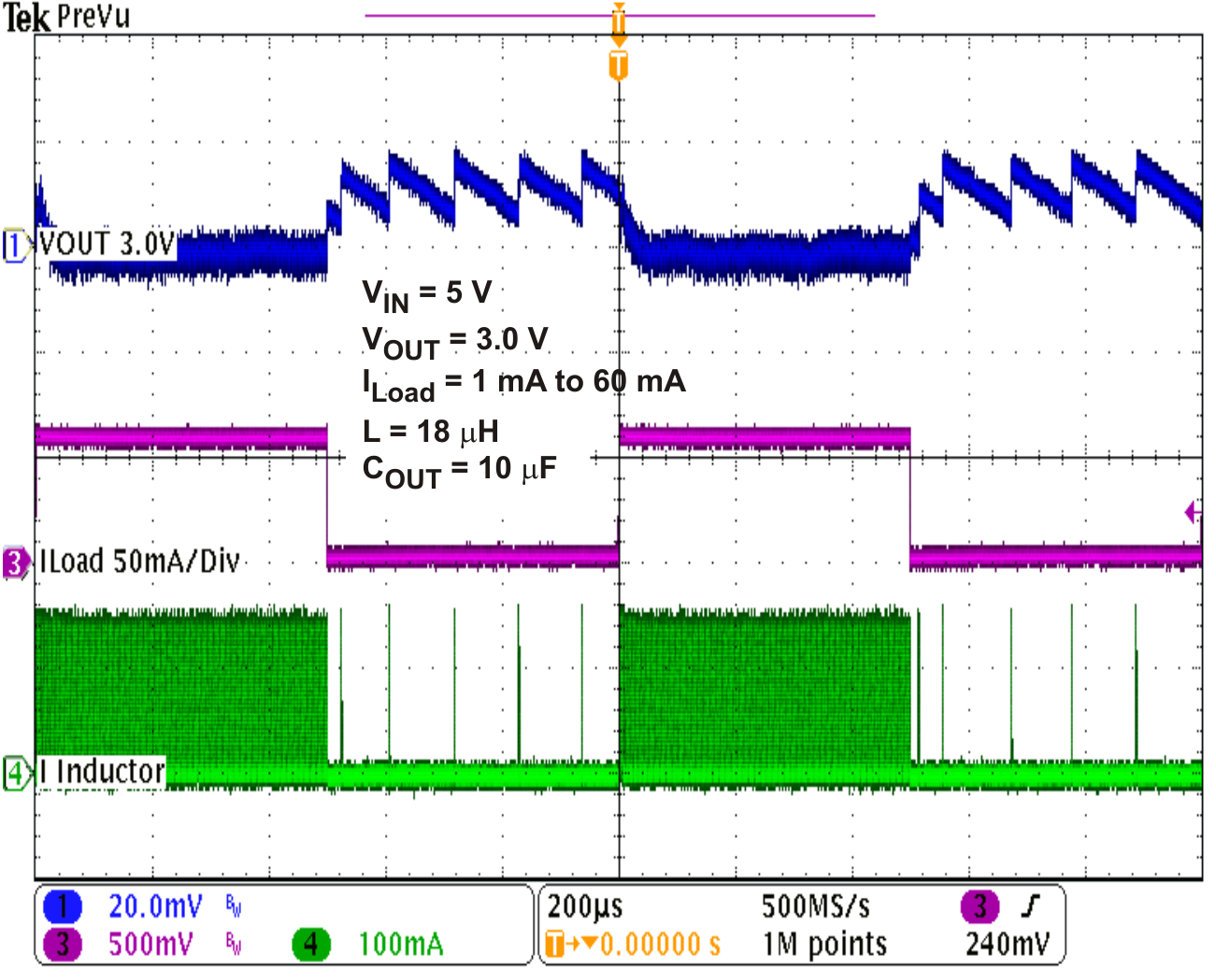
GUID-EB855807-AC00-4FB6-9BD4-5B5EBB65F449-low.pngFigure 5-6 TPS62120 Load Transient Response(VIN = 8.0 V, VOUT = 1.8 V)