SLVU641A January 2012 – November 2021 TPS54120
5.1 Layout Description
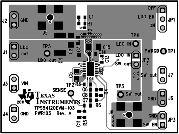
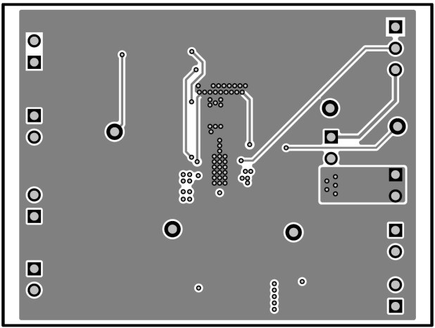
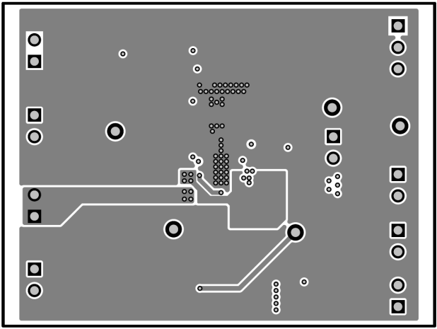
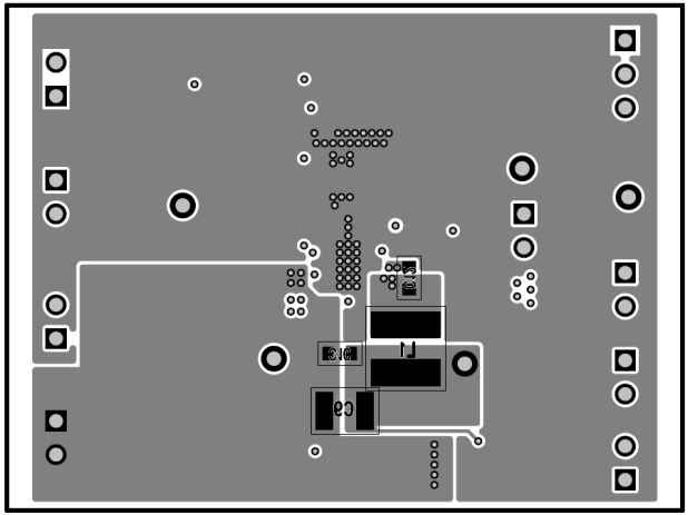
The board layout for the TPS54120 evaluation board is shown in Figure 5-1 through Figure 5-4. The board consists of four layers. It is laid out in such a way the analog ground of the LDO is shielded as much as possible from the noise of the switcher. Also, critical analog circuits such as the voltage set point divider, frequency set resistor, slow-start capacitor, and compensation components are terminated to ground using a via separate from the power ground pour. The top-side layer of the EVM is laid out in a manner typical of a user application.
The top layer contains the analog ground of the LDO and a portion of the output power ground of the SW side. The first internal layer is connected to the powerpad and the analog ground of the IC; mostly this layer is used for power dissipation. Only a few traces are implemented on this layer such as the LDO enable and the PWRGD test point trace.
The second internal layer is mostly used for analog ground as well. For shielding the LDO ground from the switch node noise, a small isolated power ground plane is made in the center of this layer to reduce capacitive coupling with analog ground. This layer also contains the input voltage trace of the switcher connecting the input capacitor and the connector J3.
About one quarter of the bottom layer contains the main input power ground trace. The inductor (L1) and the output capacitors (C9, C10) of the switcher are located in the center of the layer. The remaining surface area is connected to the analog ground of the top and the internal layers through vias. Some of these vias are directly under the TPS54120 device to provide a thermal path from the top-side ground plane to the internal and bottom-side ground plane.
The input decoupling capacitor of the SW (C5) is located as close as possible to the IC. PVIN and VIN are connected together in this EVM, and then through vias, they are connected to the input voltage trace in the second internal layer. Whereas, the decoupling capacitor ground is connected through vias to the bottom layer. The compensation and the soft-start capacitors (C6, C7, and C8), the CLK/RT resistor (R3), and the SW feedback resistor (R6) are grounded to a power-ground trace in the center of the top layer. This helps shield them from noises of the high current ground plane.
The inductor (L1), the boot capacitor (C12), and the output capacitors of the SW (C9, C10) are placed on the bottom layer of the board to shield the switching noise into the LDO side. However, the boot capacitor (C12) and the inductor (L1) are connected through vias directly into the PH pin of the IC. This connects them as close as possible to the PH pin and reduces parasitic inductance of long traces. Also, the noise reduction capacitor (C13) is placed as close as possible to the IC.
The input of the LDO is connected to the output of the switcher using a shorting jumper and a long trace parallel with the trace that connects the ground on the LDO with the ground of the switcher. Critical analog ground of the LDO circuits such as the voltage set point divider, the LDO input, and output capacitors are terminated to ground using a wide ground trace separate from the power ground pour. In addition, the input and the output LDO capacitors are kept close to the IC. The voltage divider network of the LDO ties to the LDO output voltage at the copper of the LDO output trace.
 Figure 5-1 Top Side Silkscreen and Routing
 Figure 5-2 Second Layer (Internal) Routing
 Figure 5-3 Third Layer (Internal) Routing
 Figure 5-4 Bottom Layer Silkscreen and Routing