SLVU641A January   2012  – November 2021 TPS54120


  1.   Trademarks
  2. 1Background
  3. 2Setup
    1. 2.1 Input and Output Connections and Jumper Descriptions
    2. 2.2 Modifications
      1. 2.2.1 SW Output Voltage Setpoint
      2. 2.2.2 LDO Output Voltage Setpoint
      3. 2.2.3 Switcher Slow-Start Time
      4. 2.2.4 LDO Start-Up
    3. 2.3 Equipment Interconnect
  4. 3Operation
  5. 4Test Results
    1. 4.1 Output Voltage Ripple
    2. 4.2 Output Noise
    3. 4.3 Output Turn-On
    4. 4.4 Load Transient
    5. 4.5 Efficiency
    6. 4.6 Thermal Characteristic
  6. 5Board Layout
    1. 5.1 Layout Description
  7. 6Schematic
  8. 7Bill of Materials
  9. 8Revision History

Output Voltage Ripple

Figure 4-1 shows the output voltage ripple of the LDO and SWITCHER converter for the TPS54120EVM with VIN = 12 V, SW OUT = 4.1 V, LDO OUT = 3.3 V, IOUT = 400 mA, Fswitching = 480 kHz.
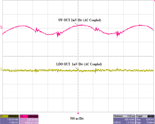
GUID-50C2B3E0-9726-4DF7-9530-4108E4053DAD-low.gifFigure 4-1 Output Voltages of Both the SW and LDO with a 400-mA Load