SLVU641A January   2012  – November 2021 TPS54120


  1.   Trademarks
  2. 1Background
  3. 2Setup
    1. 2.1 Input and Output Connections and Jumper Descriptions
    2. 2.2 Modifications
      1. 2.2.1 SW Output Voltage Setpoint
      2. 2.2.2 LDO Output Voltage Setpoint
      3. 2.2.3 Switcher Slow-Start Time
      4. 2.2.4 LDO Start-Up
    3. 2.3 Equipment Interconnect
  4. 3Operation
  5. 4Test Results
    1. 4.1 Output Voltage Ripple
    2. 4.2 Output Noise
    3. 4.3 Output Turn-On
    4. 4.4 Load Transient
    5. 4.5 Efficiency
    6. 4.6 Thermal Characteristic
  6. 5Board Layout
    1. 5.1 Layout Description
  7. 6Schematic
  8. 7Bill of Materials
  9. 8Revision History

Schematic

Figure 6-1 is the schematic for the TPS54120 evaluation board.
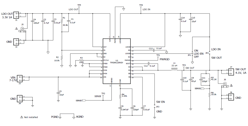
GUID-B6083013-9895-4E58-8043-E2CF90A12238-low.gifFigure 6-1 Schematic