SLVUBE6C November   2018  – July 2021 TPS56339


  1.   Trademarks
  2. 1Introduction
  3. 2Performance Specification Summary
  4. 3Modifications
    1. 3.1 Output Voltage Set Point
    2. 3.2 Adjustable UVLO
  5. 4EVM Photos
  6. 5Test Setup and Results
    1. 5.1  Input/Output Connections
    2. 5.2  Start-Up Procedure
    3. 5.3  Efficiency
    4. 5.4  Output Voltage Load Regulation
    5. 5.5  Output Voltage Line Regulation
    6. 5.6  Load Transients
    7. 5.7  Voltage Ripple
    8. 5.8  Powering Up
    9. 5.9  Powering Down
    10. 5.10 Output Short Protection and Recovery
    11. 5.11 Thermal Performance
  7. 6Board Layout
    1. 6.1 Layout
  8. 7Schematic and List of Materials
    1. 7.1 Schematic
    2. 7.2 List of Materials
  9. 8Revision History

Output Voltage Set Point

The voltage divider, R6 and R7, is used to set the output voltage. To change the output voltage of the EVM, it is necessary to change the value of resistor R6. Changing the value of R6 can change the output voltage above 0.8 V. The value of R6 for a specific output voltage can be calculated using Equation 1. Use 10 kΩ for R7.

Equation 1. GUID-A6D6A79F-D167-4E0F-801B-56EE42E317D2-low.gif

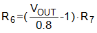
Table 3-1 lists the R6 and R7 values for some common output voltages. Note that VIN must be in a range so that the minimum on-time is greater than 55 ns. The values in Table 3-1 are standard values, not the exact value calculated using Equation 1.

Be noted that the voltage rate of the output capacitors is only 16 VDC, higher voltage rate capacitors should be used when the configured output voltage is equal or higher than 12V.

Table 3-1 Recommended Component Values
OUTPUT VOLTAGE(1)
(V)
R6(2)
(kΩ)
R7
(kΩ)
L1(3)
(µH)
COUT(4)
(µF)
Range of L1·COUT_E(5)
(μH×μF)
1.053.1610.01.52×2248 to 188
1.812.410.02.22×2264 to 250
2.521.510.03.32×2287 to 334
3.331.610.04.72×22107 to 404
552.310.05.62×2293 to 334
1214010.06.83×2245 to 137
Please use the recommended L1 and COUT combination of the higher and closest output rail for the unlisted output rails.
R6 = 0 Ω for VOUT = 0.8 V.
Inductance values are calculated based on VIN = 19 V, but they can also be used for other input voltages. User can calculate their preferred inductance value per TPS56339 datasheet.
The COUT is the sum of nominal output capacitance. Two 22-uF, 0805, 16VDC capacitors are recommended for VOUT ≤ 5V, three 22-uF, 0805, 25VDC capacitors are recommended for VOUT > 5V.
The COUT_E is the effective value after derating, the value of L1·COUT_E should be within in the range.