SLVUC22 July 2021 TPS62912 , TPS62913
2.2 Ripple Measurement
The extremely low noise and low ripple levels of the TPS6291x necessitate a low-noise test setup for accurately measuring the output voltage ripple. The SMA connectors, J4 and J5, should be used to measure the output voltage ripple, before and after the second LC filter. Do not use a normal 10x oscilloscope probe with a high-impedance termination to the oscilloscope. Instead, connect the SMA connector directly to the oscilloscope with a coaxial (coax) cable through a DC blocker. A DC blocker enables the use of the smallest V/div setting on the oscilloscope to view the ripple. To prevent noise pickup and block reflections on the coax cable, the oscilloscope should be set to full bandwidth (BW) and DC coupling with a 50-Ω termination.
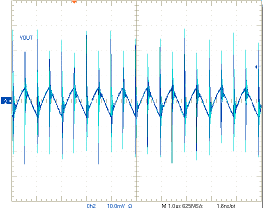
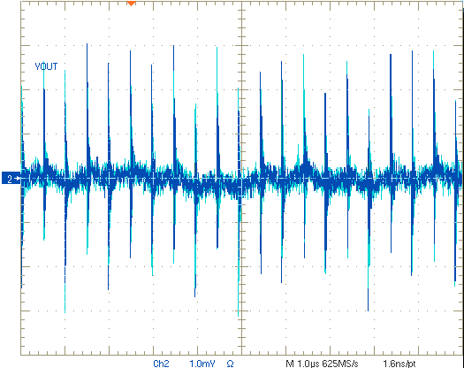
Figure 2-1 and Figure 2-2 show the correct measurement settings and output voltage ripple result. The measurement at J4 is prior to the ferrite bead filter, and the measurement at J5 is after the ferrite bead filter.

VIN = 5 V, VOUT = -5 V, IOUT = 1000 mA, FSW = 1 MHz, Full BW, DC Coupling, 50-Ω Termination With DC Blocker
Figure 2-1 Output Voltage Ripple, Measured at J4 (First LC Filter)
VIN = 5 V, VOUT = -5 V, IOUT = 1000 mA, FSW = 1 MHz, Full BW, DC Coupling, 50-Ω Termination With DC Blocker
Figure 2-2 Output Voltage Ripple, Measured at J5 (After Ferrite Bead)