SLVUC27 January 2021 TPS61094
2.2.1 Boost Converter with Bypass
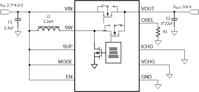
In this section, it shows how to set the EVM to support Boost converter with bypass application. The sketch schematic is shown in Figure 2-1, while the jumper configuration is shown in Table 2-2
 Figure 2-1
Boost Converter with Bypass
Figure 2-1
Boost Converter with BypassTable 2-2 Jumpers Configuration for Boost Converter with
Bypass
| Reference Designator | Description | Configuration |
|---|---|---|
| JP1, JP2 | Short 1-2 :connect the SUP pin to the Vin port Short 2-3: connect the SUP pin to the SUP port |
Short 1-2 |
| JP3 | Sup termination voltage selection | - |
| JP4 | Changing current selection | - |
| JP5 | Output voltage target selection | At mark 3.6 V |
| J11, J12 | Operating mode selection pin. The MODE pin and EN pin work together to set device operation mode. | Set High to select auto Buck or boost mode |