SLVUCG9 October 2022 TPS36-Q1
4.2 EVM Test Points
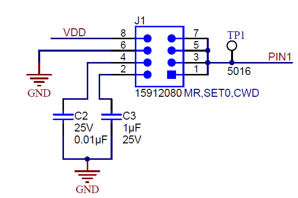
Test points are placed throughout the board and are used to verify pin functionality. Each device configuration option letter has different pinouts, so each test point can serve different purposes depending on the chosen IC. For example, test point 1 (TP1) is used to monitor pin 1, but the functionality of pin 1 varies between MR, SET0, and CWD as seen in Figure 4-1. Jumpers can be used with shunt jumpers to connect two pins together in order to serve multiple testing purposes. For example, connecting pins 7-8 of jumper J1 connects pin 1 to VDD, a logic high, and connecting pins 5-6 of jumper J1 connects pin 1 to GND, a logic low. Pins can also be connected to delay capacitors via the jumpers, and these connections can be used to adjust programmable timeout periods.
 Figure 4-1 Schematic Closeup