SLVUCQ6 july 2023 TPS7H2211-SEP
2.1 EVM Connectors and Test Points
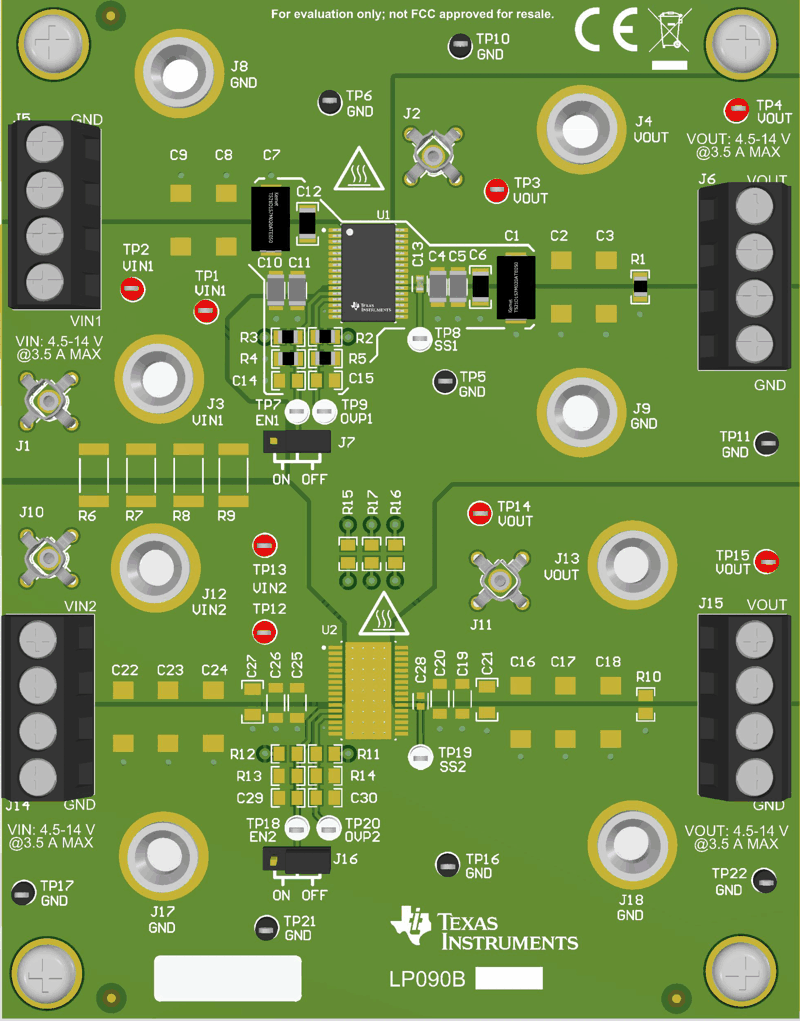
 Figure 2-1 TPS7H2211EVM 3D Rendering (Top)
Table 2-1 Summary of Connectors and Test Points
| Reference Designator | Function | |
|---|---|---|
| J3, J5 (pins 3 & 4) | VIN1 | Input Voltage and Current for U1 |
J8, J5 (pins 1 & 2) | GND | |
| J12, J14 (pins 1 & 2) | VIN2 | Input Voltage and Current for U2 |
| J17, J14 (pins 3 & 4) | GND | |
| J4, J13, J6 (pins 3 & 4), J15 (pins 3 & 4) | VOUT | Output Voltage and Current for Board |
| J9, J18, J6 (pins 1 & 2), J15 (pins 1 & 2) | GND | |
J1, TP1, TP2 | VIN1 | Test Point |
J10, TP12, TP13 | VIN2 | |
J2, J11, TP3, TP4, TP14, TP15 | VOUT | |
TP5, TP6, TP10, TP11, TP16, TP17, TP21, TP22 | GND | |
TP8 | SS1 | |
TP19 | SS2 | |
TP7 | EN1 | |
TP18 | EN2 | |
TP9 | OVP1 | |
TP20 | OVP2 | |
J7 | VIN1-EN1-GND | Shunt for mode selection |
J16 | VIN2-EN2-GND | |