SLVUD99 May   2025 TPS7H4013-SEP


  1.   1
  2.   Description
  3.   Features
  4.   4
  5. 1Evaluation Module Overview
    1. 1.1 Introduction
    2. 1.2 Kit Contents
    3. 1.3 Specification
    4. 1.4 Device Information
  6. 2Hardware
    1. 2.1 Setup
      1. 2.1.1 Transient Load Circuit
    2. 2.2 Connector Descriptions
    3. 2.3 Best Practices
  7. 3Implementation Results
    1. 3.1 Default Configuration Results
    2. 3.2 Soft Startup
    3. 3.3 Voltage Ripple on VOUT
    4. 3.4 Load Step
    5. 3.5 Frequency Response
  8. 4Hardware Design Files
    1. 4.1 Schematics
    2. 4.2 PCB Layouts
    3. 4.3 Bill of Materials (BOM)
  9. 5Additional Information
    1. 5.1 Trademarks
  10. 6Related Documentation

PCB Layouts

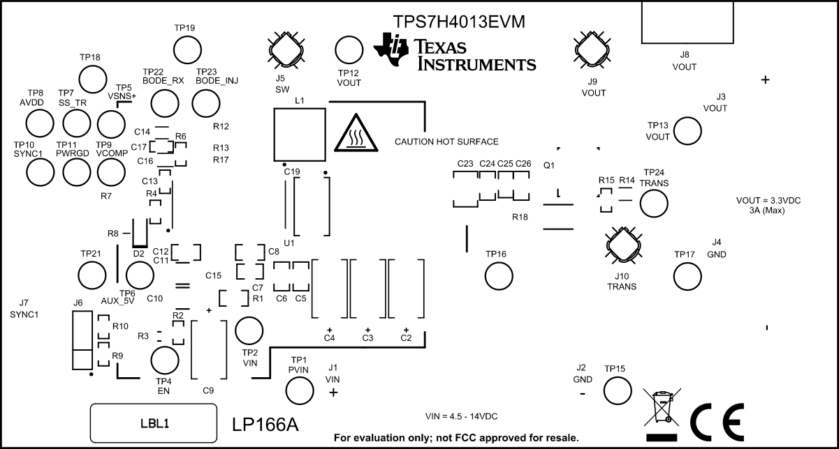
TPS7H4013EVM Top OverlayFigure 4-2 Top Overlay
TPS7H4013EVM Top Solder MaskFigure 4-3 Top Solder Mask
TPS7H4013EVM Layer 1 (Top)Figure 4-4 Layer 1 (Top)
TPS7H4013EVM Layer 2Figure 4-5 Layer 2
TPS7H4013EVM Layer 3Figure 4-6 Layer 3
TPS7H4013EVM Layer 4 (Bottom)Figure 4-7 Layer 4 (Bottom)
TPS7H4013EVM Bottom Solder MaskFigure 4-8 Bottom Solder Mask
TPS7H4013EVM Bottom OverlayFigure 4-9 Bottom Overlay
TPS7H4013EVM Drill DrawingFigure 4-10 Drill Drawing