SLYT848 February 2024 LM74700-Q1 , LM74900-Q1
3 Typical application circuits for power-supply ORing
ORing circuits are popular in automotive subsystems such as infotainment, body control modules, advanced driver assistance systems and lighting modules; they provide redundancy and reliability in case of a power-supply failure or disconnection. Figure 2 shows different ORing topologies using ideal diode controller ICs combined with external N-channel MOSFETs.
An effective ORing solution needs to be extremely fast in order to limit the duration and amount of reverse current in case one of the supplies fails. The ideal diode controllers in an ORing configuration constantly sense the voltage difference between the anode and cathode pins, which are the voltage levels at the power sources (VIN1, VIN2) and the common-load (VOUT) point, respectively. A fast comparator shuts down the gate drive through a fast pulldown – within microseconds as soon as VIN – VOUT falls below a designated reverse threshold, typically a few millivolts. Along with a fast reverse-current detection comparator, TI ideal diode controllers have a linear gate regulation scheme that ensures zero DC reverse current in the event of an input supply loss.
 Figure 2 Typical ORing topologies using
ideal diode controllers.
Figure 2 Typical ORing topologies using
ideal diode controllers.Few subsystems require disconnecting the load from the power supplies to achieve low quiescent current or to protect the system from fault conditions. Topology No. 2 in Figure 2 shows a typical application circuit for a dual-supply input ORing with a common load disconnect control using TI’s LM7480-Q1 and LM7470-Q1 devices. FET Q1 and Q2, driven by the LM7470-Q1 and LM7480-Q1, respectively, provide ORing functionality, whereas the Q3 FET driven by the LM7480-Q1 can isolate the load from power supplies. When VIN1 is greater than VIN2, the independent control of FETs by the LM7480-Q1 allows Q2 to block reverse current, while Q3 remains on, connecting VIN1 to VOUT.
Topology No. 3 in Figure 2 shows a typical application circuit for ORing with load disconnect functionality for individual rails, thus allowing system designers to assign different load disconnect criteria for each rail.
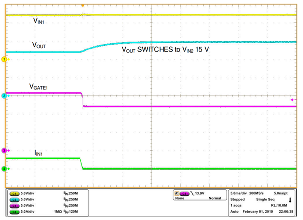
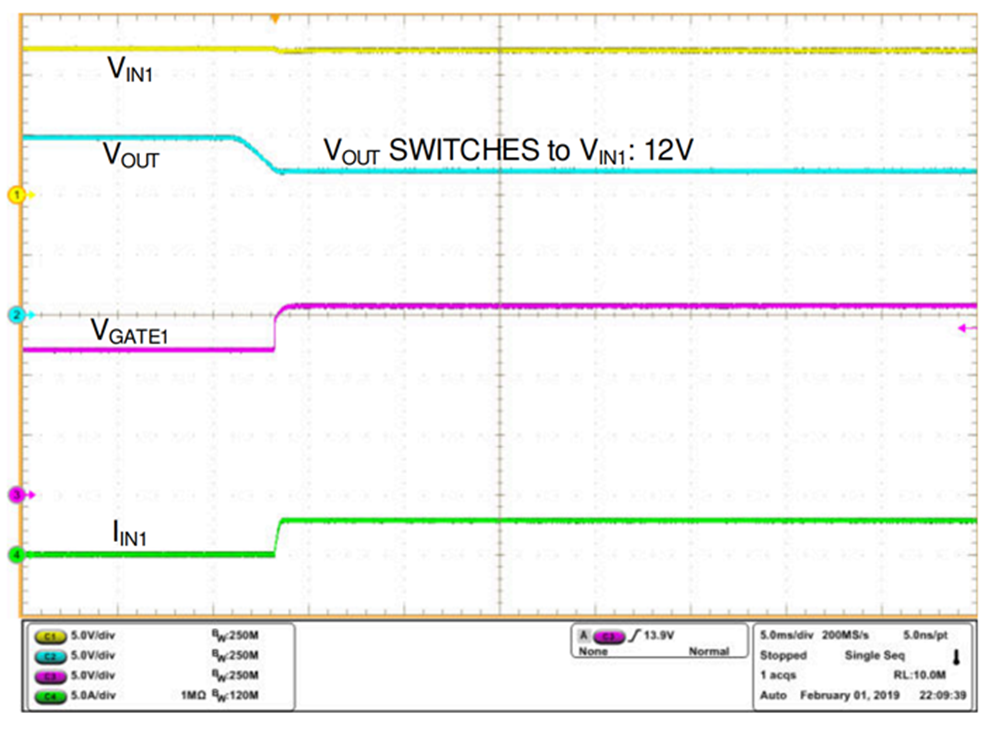
Figure 3 and Figure 4 shows power-supply ORing switchover performance between two power-supply rails where VIN1 = 12V and VIN2 = 15V.
 Figure 3 Supply switchover from VIN1 to
VIN2.
 Figure 4 Supply switchover from VIN2 to
VIN1.