SLYY222 November 2023 ADC12DJ5200RF , ADS127L11 , BQ79731-Q1 , REF35 , REF70 , TPS62912 , TPS62913 , TPS7A20 , TPS7A94 , TPSM82912 , TPSM82913
- 1
- Overview
- At a glance
- Noise and ADCs
- Defining noise and precision in a power architecture
- Innovations in low-noise and low-power voltage references
- Innovations in ultra-low-noise voltage references
- Improving noise and thermal performance with simplified power architectures
- High-current low noise with LDO supply rails
- Innovations in precision battery monitoring
- Conclusion
- Additional resources
High-current low noise with LDO supply rails
The biggest intrinsic noise source for an LDO is its internal voltage reference. In order to reduce noise and improve overall system performance, a variety of LDOs in the TI portfolio have incorporated a noise-reduction feature with a NR pin. Adding a capacitor (CNR/SS) to the NR pin creates a resistor-capacitor filter with internal resistance at the VREF node, as shown in Figure 12.
 Figure 12 N-channel metal-oxide
semiconductor LDO with an NR/SS pin.
Figure 12 N-channel metal-oxide
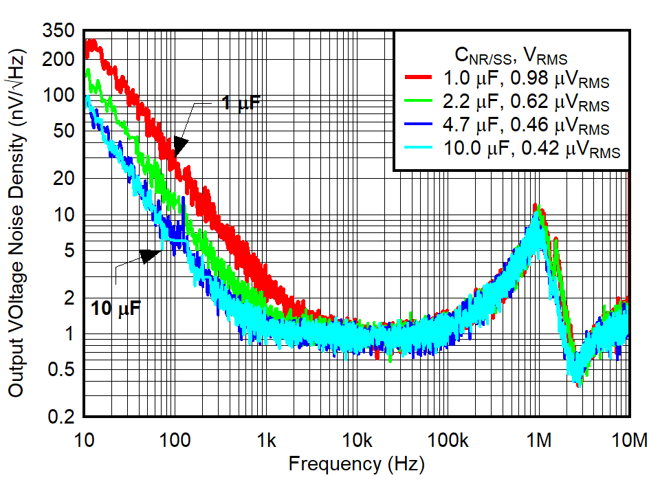
semiconductor LDO with an NR/SS pin.Newer LDOs implement a highly accurate, high-precision and low-noise current source, followed by an error amplifier. Implementing a unity-gain configuration also ensures low noise over the entire output range. A great example of one of these high-accuracy low-noise LDOs is the TPS7A94, which can achieve 0.46 μVRMS over a 10-Hz to 100-kHz bandwidth. Figure 13 shows the output noise density and the impact of increasing CNR/SS from 1 µF to 10 µF.

| VOUT = 3.3 V | CIN = COUT = 10 μF |
| IOUT = 500 mA | 10 Hz ≤ fSW ≤100 kHz |
The combination of features that the TPS7A94 possesses represents a new generation of low-noise LDOs capable of achieving excellent voltage accuracy and ultra-low noise, which is important when the TPS7A94 is the primary power supply for a high-resolution signal chain, since higher-resolution ADCs are more sensitive to noise. In a typical application, shown in Figure 14, the TPS7A94 is the main power supply for the ADC, operational amplifier, clock and external voltage reference, which are high-performance devices. The goal of this signal chain is to maximize the total harmonic distortion, signal-to-noise ratio and gain error of the ADS127L11 by using the ultra-low input current noise with the low 1/f noise of the TPH210 and REF70. The low noise and high PSRR of the TPS7A94 provide a clean supply line that limits any noise that could couple into the active circuitry of the TPS210, ADC127L11 and REF70 and degrade performance.
 Figure 14 TPS7A94 powering a signal
chain.