SNAS513F August 2011 – November 2015 LM48560
PRODUCTION DATA.
- 1 Features
- 2 Applications
- 3 Description
- 4 Revision History
- 5 Pin Configuration and Functions
- 6 Specifications
- 7 Parameter Measurement Information
- 8 Detailed Description
- 9 Application and Implementation
- 10Power Supply Recommendations
- 11Layout
- 12Device and Documentation Support
- 13Mechanical, Packaging, and Orderable Information
6 Specifications
6.1 Absolute Maximum Ratings
over operating free-air temperature range (unless otherwise noted)(1)| MIN | MAX | UNIT | |||
|---|---|---|---|---|---|
| VDD | Supply voltage(2) | 6 | V | ||
| SW | Voltage | 25 | V | ||
| VBST | Voltage | 21 | V | ||
| Input voltage | –0.3 | VDD 0.3 | V | ||
| Power dissipation(3) | Internally limited | ||||
| TJ | Junction temperature | 150 | °C | ||
| Tstg | Storage temperature | –65 | 150 | °C | |
(1) Stresses beyond those listed under Absolute Maximum Ratings may cause permanent damage to the device. These are stress ratings only, which do not imply functional operation of the device at these or any other conditions beyond those indicated under Recommended Operating Conditions. Exposure to absolute-maximum-rated conditions for extended periods may affect device reliability.
(2) All voltages are measured with respect to the ground pin, unless otherwise specified.
(3) The maximum power dissipation must be derated at elevated temperatures and is dictated by TJMAX, θJA, and the ambient temperature, TA. The maximum allowable power dissipation is PDMAX = (TJMAX –TA) / θJA or the given in Absolute Maximum Ratings, whichever is lower.
6.2 ESD Ratings
| VALUE | UNIT | |||
|---|---|---|---|---|
| V(ESD) | Electrostatic discharge | Human-body model (HBM), per ANSI/ESDA/JEDEC JS-001(1) | ±2000 | V |
| Charged-device model (CDM), per JEDEC specification JESD22-C101(2) | ±500 | |||
| Machine Model(3) | ±100 | |||
(1) JEDEC document JEP155 states that 500-V HBM allows safe manufacturing with a standard ESD control process.
(2) JEDEC document JEP157 states that 250-V CDM allows safe manufacturing with a standard ESD control process.
(3) Machine model, applicable std. JESD22-A115-A.
6.3 Recommended Operating Conditions
over operating free-air temperature range (unless otherwise noted)| MIN | NOM | MAX | UNIT | ||
|---|---|---|---|---|---|
| TA | Operating free-air temperature | –40 | 85 | °C | |
| VDD | Supply voltage | 2.7 | 5.5 | V | |
6.4 Electrical Characteristics VDD = 3.6 V
The following specifications apply for RL = 1.5 μF + 10 Ω, CBST = 1 μF, CIN = 0.47 μF, CSET = 100 nF, AV = 24 dB unless otherwise specified. Limits apply for TA = 25 °C.(2)(1)| PARAMETER | TEST CONDITIONS | MIN (1) | TYP (2) | MAX (1) | UNIT | ||
|---|---|---|---|---|---|---|---|
| VDD | Supply voltage | 2.7 | 5.5 | V | |||
| IDD | Quiescent power supply current | VIN = 0 V, RL = ∞ | |||||
| ALC Enabled | 4 | 6 | mA | ||||
| ALC Disabled | 3.6 | mA | |||||
| PD | Power consumption | VOUT = 25 VP-P, f = 1 kHz | 1 | W | |||
| ISD | Shutdown current | Software Mode | 2.5 | 4.4 | µA | ||
| Hardware Mode | 0.1 | 2 | µA | ||||
| TWU | Wake-up time | From Shutdown | 15 | ms | |||
| VOS | Differential output offset voltage | AV = 24 V | 10 | 90 | mV | ||
| AV = 0 dB (Boost Disabled) | 5 | 20 | mV | ||||
| AV | Gain (Hardware Mode) | IN1 | GAIN = 0 | 0.5 | 0 | 0.5 | dB |
| GAIN = 1 | 5.5 | 6 | 6.5 | ||||
| IN2 | GAIN = 0 | 23.5 | 24 | 24.5 | |||
| GAIN = 1 | 29.5 | 30 | 30.5 | ||||
| Gain (software mode) | Boost Disabled | GAIN1 = 0, GAIN0 = 0 | –0.5 | 0 | 0.5 | dB | |
| GAIN1 = 0, GAIN0 = 1 | 5.5 | 6 | 6.5 | ||||
| GAIN1 = 1, GAIN0 = 0 | 11.5 | 12 | 12.5 | ||||
| GAIN1 = 1, GAIN0 = 1 | 17.5 | 18 | 18.5 | ||||
| Boost Enabled | GAIN1 = 0, GAIN0 = 0 | 20.5 | 21 | 21.5 | dB | ||
| GAIN1 = 0, GAIN0 = 1 | 23.5 | 24 | 24.5 | ||||
| GAIN1 = 1, GAIN0 = 0 | 26.5 | 27 | 27.5 | ||||
| GAIN1 = 1, GAIN0 = 1 | 29.5 | 30 | 30.5 | ||||
| RIN | Gain step size (software mode) | 3 | dB | ||||
| Input resistance | AV | 0 dB | 46 | 50 | 58 | kΩ | |
| 30 dB | 46 | 50 | 58 | ||||
| VOUT | Output voltage | THD+N = 1% | VP-P | ||||
| f | 200 Hz | 25 | 30 | ||||
| 1 kHz | 25 | 30 | |||||
| THD+N | Total harmonic distortion + noise | VOUT = 18 VP-P, f = 1 kHz | 0.08% | ||||
| PSRR | Power supply rejection ratio (Figure 22) |
VDD = 3.6 V + 200 mVP-P sine, Inputs = AC GND | dB | ||||
| fRIPPLE = 217 Hz | 55 | 78 | |||||
| fRIPPLE = 1 kHz | 76 | ||||||
| CMRR | Common mode rejection ratio (Figure 23) |
VCM = 200 mVP-P sine | |||||
| fRIPPLE = 217 Hz | 68 | dB | |||||
| fRIPPLE = 1k Hz | 78 | dB | |||||
| SNR | Signal-to-noise-ratio | Boost Disabled, A-weighted | 107 | dB | |||
| Boost Enabled A-weighted | 98 | dB | |||||
| εOS | Output noise | A-weighted | |||||
| AV | 24 dB | 134 | μVRMS | ||||
| 0 dB (Boost Disabled) | 16 | ||||||
| TA | Attack time | ATK1:ATK0 = 00, CSET = 100 nF | 0.83 | ms | |||
| TR | Release time | RLT1:RLT0 = 00, CSET = 100 nF | 0.5 | s | |||
| fSW | Boost converter switching frequency | 2 | MHz | ||||
| ILIMIT | Boost converter current limit | 1.5 | A | ||||
| VIH | Logic high input threshold | SHDN | 1.4 | V | |||
| VIL | Logic low input threshold | SHDN | 0.5 | V | |||
| IIN | Input leakage current | SHDN | 0.1 | 0.2 | μA | ||
(1) Datasheet min/max specification limits are ensured by design, test, or statistical analysis.
(2) Typical values represent most likely parametric norms at TA = 25 ºC, and at the Recommended Operation Conditions at the time of product characterization and are not ensured.
6.5 I2C Interface Characteristics
The following specifications apply for RPU = 1 kΩ to VDD, SW/HW = 1 (Software Mode) unless otherwise specified. Limits apply for TA = 25 °C. (2)(1)| PARAMETER | TEST CONDITIONS | MIN (2) | TYP (2) | MAX (2) | UNIT | |
|---|---|---|---|---|---|---|
| VIH | Logic Input High Threshold | SDA, SCL | 1.1 | V | ||
| VIL | Logic Input Low Threshold | SDA, SCL | 0.5 | V | ||
| SCL Frequency | 400 | kHz | ||||
| t1 | SCL Period | 2.5 | μs | |||
| t2 | SDA Setup Time | 250 | ns | |||
| t3 | SDA Stable Time | 250 | ns | |||
| t4 | Start Condition Time | 250 | ns | |||
| t5 | Stop Condition Time | 250 | ns | |||
(1) The Electrical Characteristics tables list ensured specifications under the listed Recommended Operating Conditions except as otherwise modified or specified by the Electrical Characteristics Conditions and/or Notes. Typical specifications are estimations only and are not ensured.
(2) Charge device model, applicable std. JESD22-C101-C.
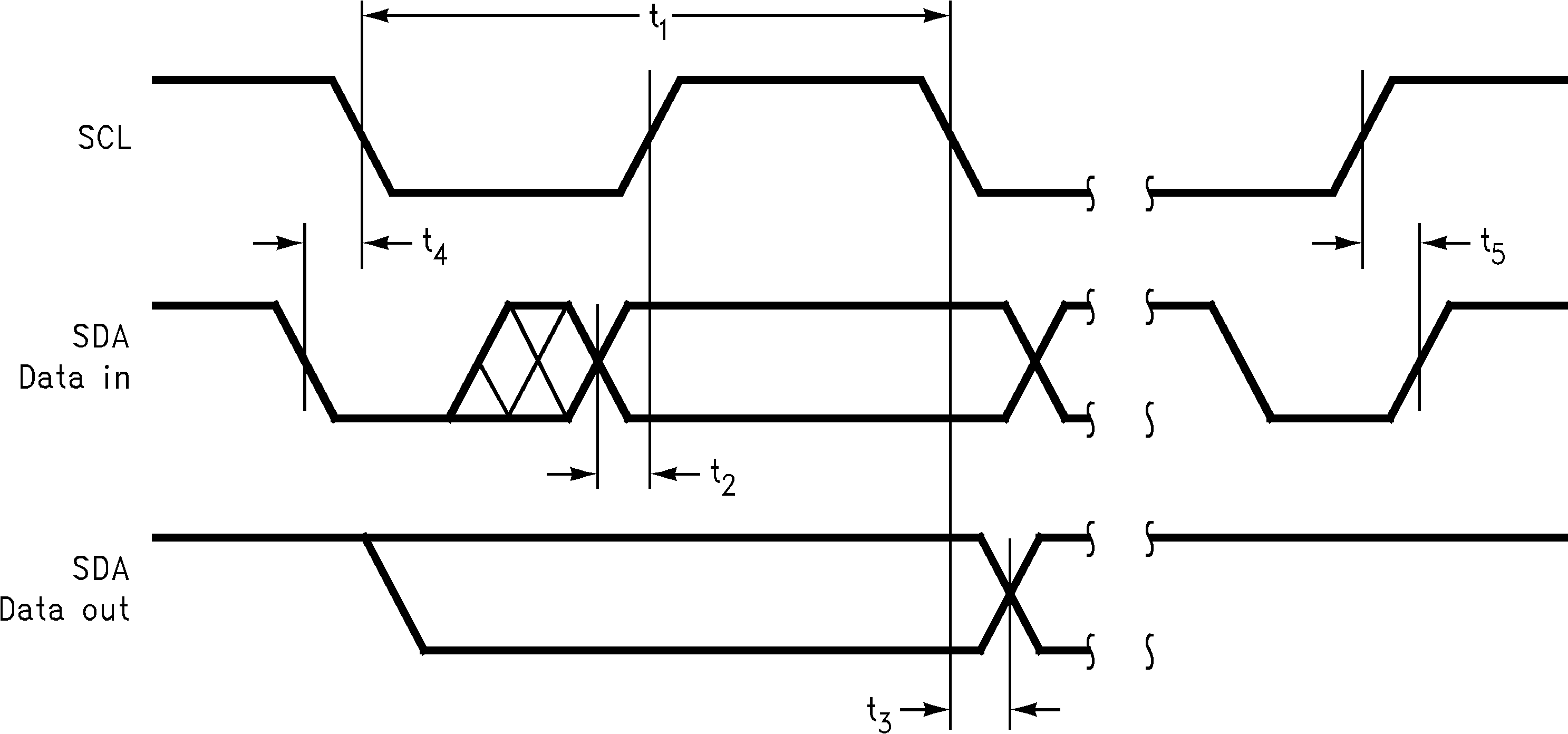 Figure 1. I2C Timing Diagram
 Figure 2. Start and Stop Diagram
6.6 Typical Characteristics
All typical performance curves are taken with conditions seen in Typical Characteristics, unless otherwise specified.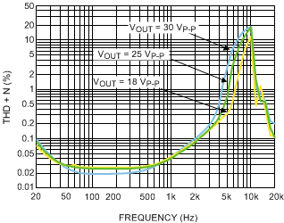 Figure 3. THD+N vs Frequency
CL = 0.6 μF, VDD = 3.6 V, Boosted, AV = 24 dB
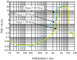 Figure 5. THD+N vs Frequency
CL = 1.5 μF, VDD = 3.6 V, Boosted, AV = 24 dB
 Figure 7. THD+N vs Frequency
VDD = 3.6 V, CL = 1 μF, VOUT = 5 VP-P
Unboosted , AV = 0 dB
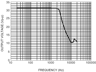 Figure 9. Output Voltage vs Frequency
CL = 1.5 μF, THD+N ≤ 1%, Boosted
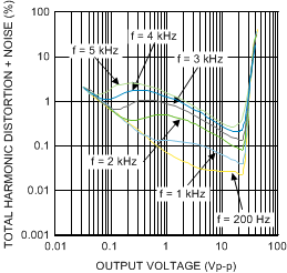 Figure 11. THD+N vs Output Voltage
CL = 0.6 μF, VDD = 3.6 V, Boosted, AV = 24 dB
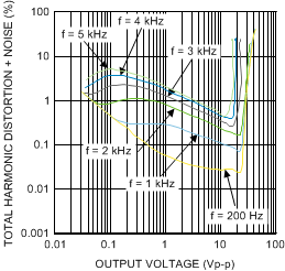 Figure 13. THD+N vs Output Voltage
CL = 1.5 μF, VDD = 3.6 V, Boosted, AV = 24 dB
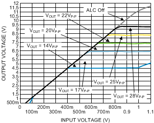 Figure 15. Input Voltage vs Output Voltage
ALC Enabled, AV = 21 dB, VDD = 3.6 V
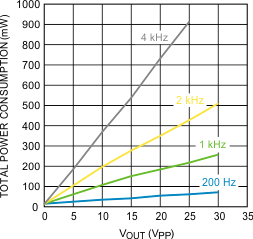 Figure 17. Total Power Consumption vs Output Voltage
VDD = 3.6 V, CL = 0.6 μF
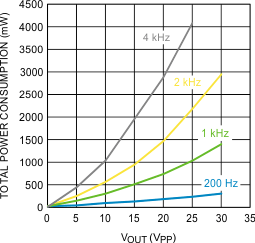 Figure 19. Total Power Consumption vs Output Voltage
VDD = 3.6 V, CL = 1.5 μF
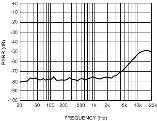 Figure 21. Power Supply Rejection Ratio vs Frequency
VRIPPLE = 200 mVP-P, VDD = 3.6 V, CL = 1.5 μF
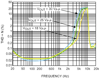 Figure 4. THD+N vs Frequency
CL = 1 μF, VDD = 3.6 V, Boosted, AV = 24 dB
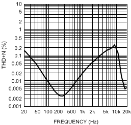 Figure 6. THD+N vs Frequency
VDD = 3.6 V, CL = 0.6 μF, VOUT = 5 VP-P
Unboosted, AV = 0 dB
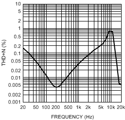 Figure 8. THD+N vs Frequency
VDD = 3.6 V, CL = 1.5 μF, VOUT = 5 VP-P
Unboosted, AV = 0 dB
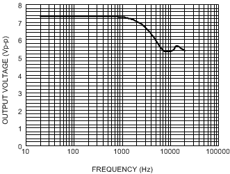 Figure 10. Output Voltage vs Frequency
CL = 1.5 μF, THD+N ≤ 1%, Unboosted
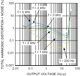 Figure 12. THD+N vs Output Voltage
CL = 1 μF, VDD = 3.6 V, Boosted, AV = 24 dB
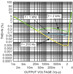 Figure 14. THD+N vs Output Voltage
CL = 1.5 μF, VDD = 3.6 V, Unboosted, AV = 0 dB
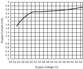 Figure 16. Supply Current vs Supply Voltage
RL = ∞
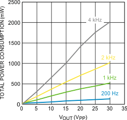 Figure 18. Total Power Consumption vs Output Voltage
VDD = 3.6 V, CL = 1 μF
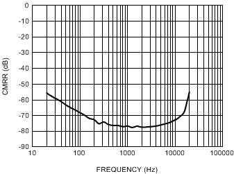 Figure 20. Common Mode Rejection Ratio vs Frequency
VCM= 200 mVP-P, CIN = 10 μF, VDD = 3.6 V, CL = 1.5 μF