SNAS717A April 2017 – October 2021 ADC12D1620QML-SP
PRODUCTION DATA
- 1 Features
- 2 Applications
- 3 Description
- 4 Revision History
- 5 Pin Configuration and Functions
-
6 Specifications
- 6.1 Absolute Maximum Ratings
- 6.2 ESD Ratings
- 6.3 Recommended Operating Conditions
- 6.4 Thermal Information
- 6.5 Converter Electrical Characteristics: Static Converter Characteristics
- 6.6 Converter Electrical Characteristics: Dynamic Converter Characteristics
- 6.7 Converter Electrical Characteristics: Analog Input/Output and Reference Characteristics
- 6.8 Converter Electrical Characteristic: Channel-to-Channel Characteristics
- 6.9 Converter Electrical Characteristics: LVDS CLK Input Characteristics
- 6.10 Electrical Characteristics: AutoSync Feature
- 6.11 Converter Electrical Characteristics: Digital Control and Output Pin Characteristics
- 6.12 Converter Electrical Characteristics: Power Supply Characteristics
- 6.13 Converter Electrical Characteristics: AC Electrical Characteristics
- 6.14 Electrical Characteristics: Delta Parameters
- 6.15 Timing Requirements: Serial Port Interface
- 6.16 Timing Requirements: Calibration
- 6.17 Quality Conformance Inspection
- 6.18 Timing Diagrams
- 6.19 Typical Characteristics
-
7 Detailed Description
- 7.1 Overview
- 7.2 Functional Block Diagram
- 7.3 Feature Description
- 7.4 Device Functional Modes
- 7.5
Programming
- 7.5.1
Control Modes
- 7.5.1.1
Non-ECM
- 7.5.1.1.1 Dual-Edge Sampling Pin (DES)
- 7.5.1.1.2 Non-Demultiplexed Mode Pin (NDM)
- 7.5.1.1.3 Dual Data-Rate Phase Pin (DDRPh)
- 7.5.1.1.4 Calibration Pin (CAL)
- 7.5.1.1.5 Low-Sampling Power-Saving Mode Pin (LSPSM)
- 7.5.1.1.6 Power-Down I-Channel Pin (PDI)
- 7.5.1.1.7 Power-Down Q-Channel Pin (PDQ)
- 7.5.1.1.8 Test-Pattern Mode Pin (TPM)
- 7.5.1.1.9 Full-Scale Input-Range Pin (FSR)
- 7.5.1.1.10 AC- or DC-Coupled Mode Pin (VCMO)
- 7.5.1.1.11 LVDS Output Common-Mode Pin (VBG)
- 7.5.1.2 Extended Control Mode
- 7.5.1.1
Non-ECM
- 7.5.1
Control Modes
- 7.6 Register Maps
- 8 Application Information Disclaimer
- 9 Power Supply Recommendations
- 10Layout
- 11Device and Documentation Support
- 12Mechanical, Packaging, and Orderable Information
6.16 Timing Requirements: Calibration
over operating free-air temperature range (unless otherwise noted)The following specifications apply after calibration for VA = VDR = VTC = VE = 1.9 V; I and Q channels AC-coupled, FSR pin = high; CL = 10 pF; differential AC-coupled sine wave input clock, fCLK = 1.6 GHz at 0.5 VP-P with 50% duty cycle; VBG = floating; non-extended control mode; Rext = Rtrim = 3300 Ω ±0.1%; analog signal source impedance = 100-Ω differential; 1:2 demultiplex non-DES mode; I and Q channels; duty-cycle stabilizer on.(1)(2)
| PARAMETER | TEST CONDITIONS | SUB-GROUPS | MIN | NOM(2) | MAX | UNIT | |
|---|---|---|---|---|---|---|---|
| tCAL | Calibration cycle time | Non-ECM | 4.1 × 10⁷ | Clock Cycles | |||
| ECM; CSS = 0b | |||||||
| ECM; CSS = 1b | |||||||
| tCAL_L | CAL pin low time | See Figure 6-8, note (3) | [9, 10, 11] | 1280 | Clock Cycles | ||
| tCAL_H | CAL pin high time | See Figure 6-8, note (3) | [9, 10, 11] | 1280 | Clock Cycles | ||
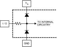
(1) The analog inputs are protected as shown below. Input voltage magnitudes beyond
the Absolute Maximum Ratings may damage this device.
(2) Typical figures are at TA = 25°C, and represent most likely parametric norms. Test limits are ensured to Texas Instrument's average outgoing quality level (AOQL).
(3) This parameter is specified by design and/or characterization and is not tested in production.