SNLA431 January 2024 DP83TC812R-Q1 , DP83TC812S-Q1
- 1
- Trademarks
- 1Preface
- Notational Conventions
- 2Related Documentation
- 3Support Resources
-
4Troubleshooting the PHY Application
- 4.1 Schematic and Layout Checklist
- 4.2 Verify Successful Power-up of PHY
- 4.3 Peripheral Pin Checks
- 4.4 Register Dump Comparison
- 4.5 Verifying Strap Configurations
- 4.6 Check the MDI Signal
- 4.7 Link Up Failed Common Issues
- 4.8 Signal Quality Check
- 4.9 Power Up Timing
- 4.10 Loopback Testing
- 4.11 Debugging the MAC Interface
- 4.12 Verify Open Alliance PMA Compliance
- 4.13 Tools and References
- 5Conclusion
4.11 Debugging the MAC Interface
The most common cause of MAC interface communication failures is incorrectly setting the desired MAC interface mode. Link can be up but a ping command fails if, for example, SGMII mode is enabled but the PCB is designed for RGMII communication. Please see the strapping tool of the DP83TC812 Schematic Checklist to confirm the correct MAC interface mode is selected. MAC mode can also be selected by writing to registers 0x600[3], 0x608[9], 0x648[6].
Reduced Gigabit Media Independent Interface (RGMII)
The signals used for the RGMII protocol are shown below:
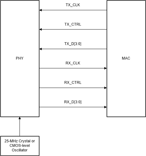 Figure 4-9 RGMII Signaling
The RGMII protocol has certain timing constraints which must be met for data to be properly received. These timing constraints are shown below in Table 4-9. Namely, a minimum of 1ns setup and 1ns hold time must be maintained at the input of the receiver. To meet this requirement, some amount of skew must be introduced between the clock and data signals. This skew can be introduced either by the MAC, the PHY, or as part of the PCB trace lengths. The DP83TC812 has two modes, align and shift mode, for both RX and TX signals. These modes are selected by bootstrap or can be adjusted in register 0x602. Note if shift mode is enabled on the PHY TX signals, the MAC transmits the data without skew. Similarly, if align mode is chosen on the PHY RX signals, the MAC must be set to RX shift mode. Table 4-8 shows the correct MAC and PHY RGMII delay configurations.
MAC Configuration | Required PHY Configuration |
|---|---|
| RGMII Align on Rx | RGMII Shift on Rx |
| RGMII Shift on Rx | RGMII Align on Rx |
| RGMII Align on Tx | RGMII Shift on Tx |
| RGMII Shift on Tx | RGMII Align on Tx |
In RGMII RX shift mode, the PHY shifts RX_CLK ahead of RX_Data signals by roughly 3ns.
When using the PHY's TX shift mode, the PHY is expecting TX_CLK and TX_Data signals to be aligned at its pins, and the data is shifted internally.
Reference waveforms below show the effect of enabling shift or align mode on RX_D0 signal.
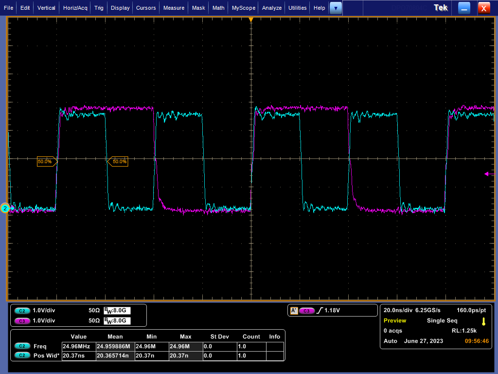 Figure 4-10 RX_CLK and RX_D0 Timing in RGMII Align Mode
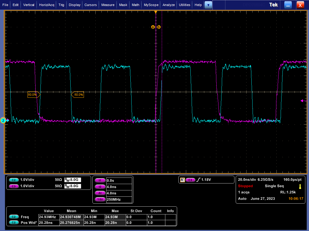 Figure 4-11 RX_CLK and RX_D0 Timing in RGMII RX Shift Mode
| PARAMETER | TEST CONDITION | Min | Typ | Max | Unit |
|---|---|---|---|---|---|
| Tcyc | TX_CLK / Clock Cycle Duration | 36 | 40 | 44 | ns |
| Tsetup(align) | TX_D[3:0], TX_CTRL setup to TX_CLK (align mode) | 1 | 2 | ns | |
Thold(align) | TX_D[3:0], TX_CTRL hold to TX_CLK (align mode) | 1 | 2 | ns |
| PARAMETER | TEST CONDITION | Min | Typ | Max | Unit |
|---|---|---|---|---|---|
| Tskew(align) | RX_D[3:0], RX_CTRL delay from RX_CLK (align mode) | -750 | 750 | ps | |
| Tskew(shift) | RX_D[3:0], RX_CTRL delay from RX_CLK (shift mode enabled, default) | 2 | ns | ||
Tcyc | RX_CLK / Clock Cycle Duration | 36 | 40 | 44 | ns |
Duty_G | RX_CLK / Duty Cycle | 45 | 50 | 55 | % |
Tr/Tf | RX_CLK / Rise, Fall Time (20% to 80% with Cload=5pF) | 1.2 | ns |
Reduced Media Independent Interface (RMII)
Two separate configurations exist when using RMII mode: RMII master mode and RMII slave mode. In RMII master mode, the PHY is provided with a 25Mhz input clock on its XI pin and outputs a 50Mhz clock signal on its RX_D3 pin (pin 23) to send to the MAC. In RMII slave mode, the PHY receives a 50Mhz clock signal on the XI pin from either the MAC or external oscillator. It is imperative that the correct RMII mode is selected via bootstrap (this cannot be changed by register write) so the PHY expects the correct reference clock (either 25Mhz or 50Mhz). Refer to the DP83TC812 Schematic Checklist strap tool to ensure the correct RMII mode is selected. Next, probe the CLKOUT pin of the PHY and ensure a 25Mhz signal is seen if RMII master mode is used and a 50Mhz signal is seen if RMII slave mode is used.
The signals used for the RMII protocol are shown below.
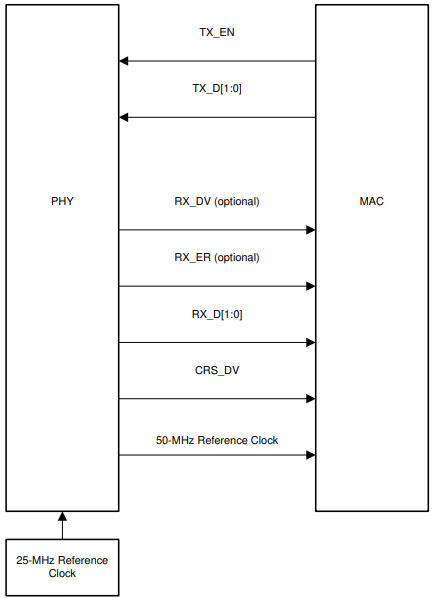 Figure 4-12 RMII Master Signaling
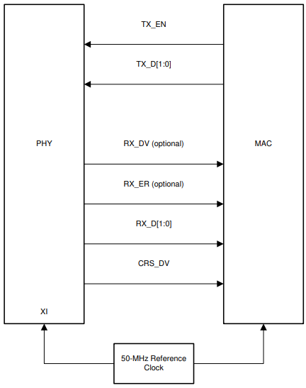 Figure 4-13 RMII Slave Signaling