SNLU301 November 2021 SN75LVPE5412 , SN75LVPE5421
- Trademarks
- 1Introduction
-
2Description
- 2.1 Redriver-Mux 5-Level I/O Control Inputs
- 2.2 Redriver-Mux Modes of Operation
- 2.3 Redriver-Mux SMBus or I2C Register Control Interface
- 2.4 Redriver-Mux Equalization Control
- 2.5 Redriver-Mux RX Detect State Machine
- 2.6 Redriver-Mux DC Gain Control
- 2.7 DS320PR412-421EVM Global Controls
- 2.8 DS320PR412-421EVM Downstream Devices Control
- 2.9 DS320PR412-421EVM Upstream Devices Control
- 2.10 Quick-Start Guide (Pin Mode)
- 2.11 Quick-Start Guide (SMBus Slave Mode)
- 3Schematics
- 4PCB Layouts
- 5Bill of Materials
3 Schematics
Figure 3-1 through Figure 3-9 show the EVM schematics.
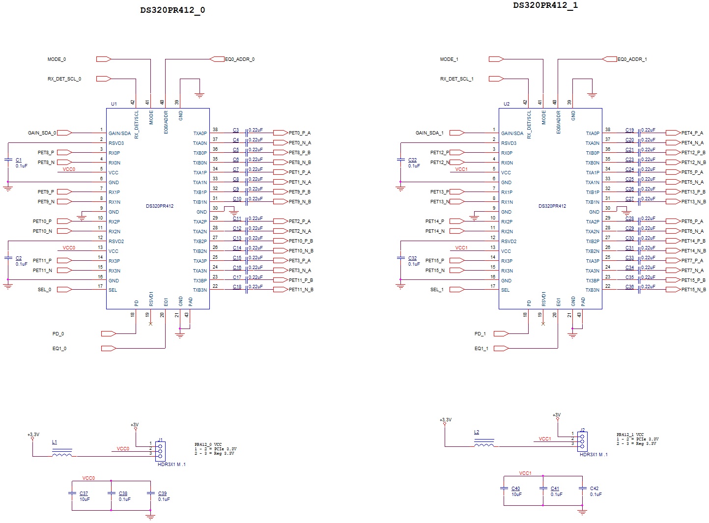 Figure 3-1 DS320PR412.
 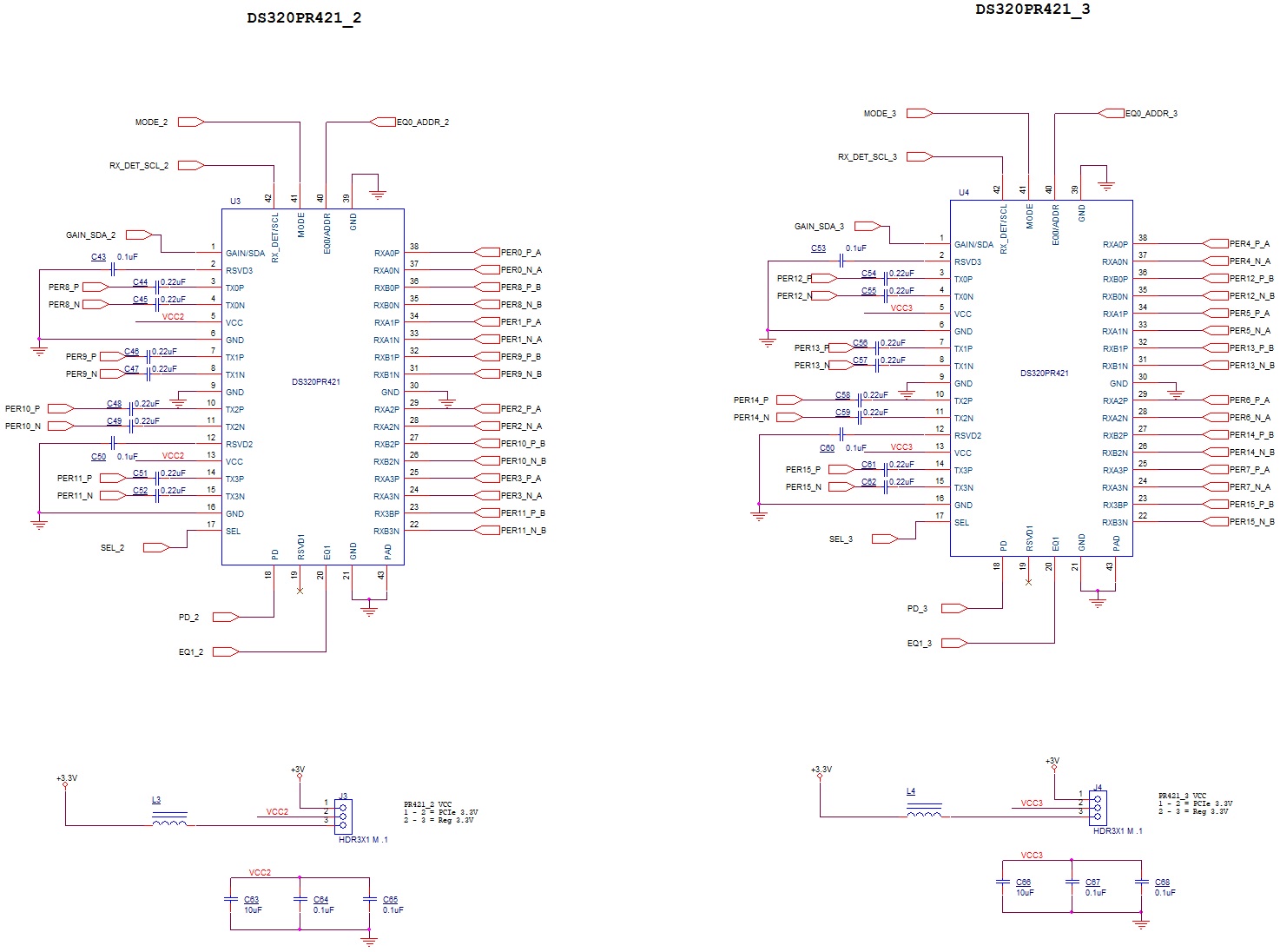 Figure 3-2 DS320PR421.
 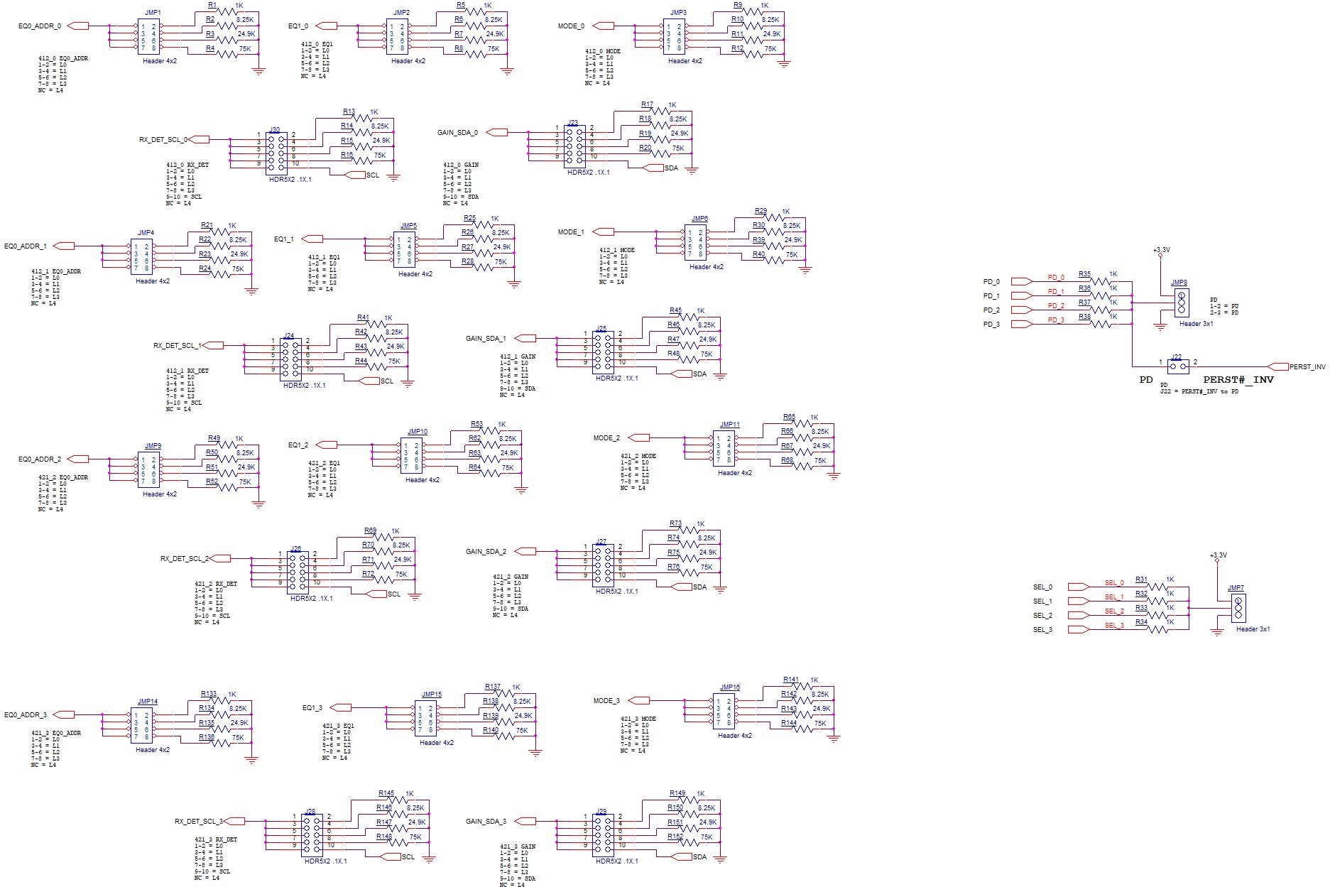 Figure 3-3 Configuration Headers.
 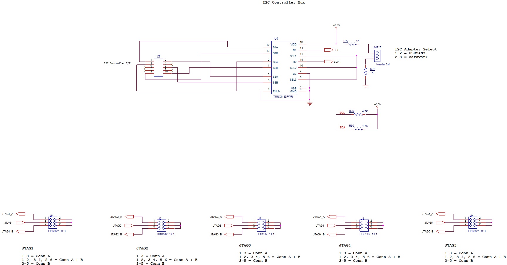 Figure 3-4 I2C Adapter Selection.
 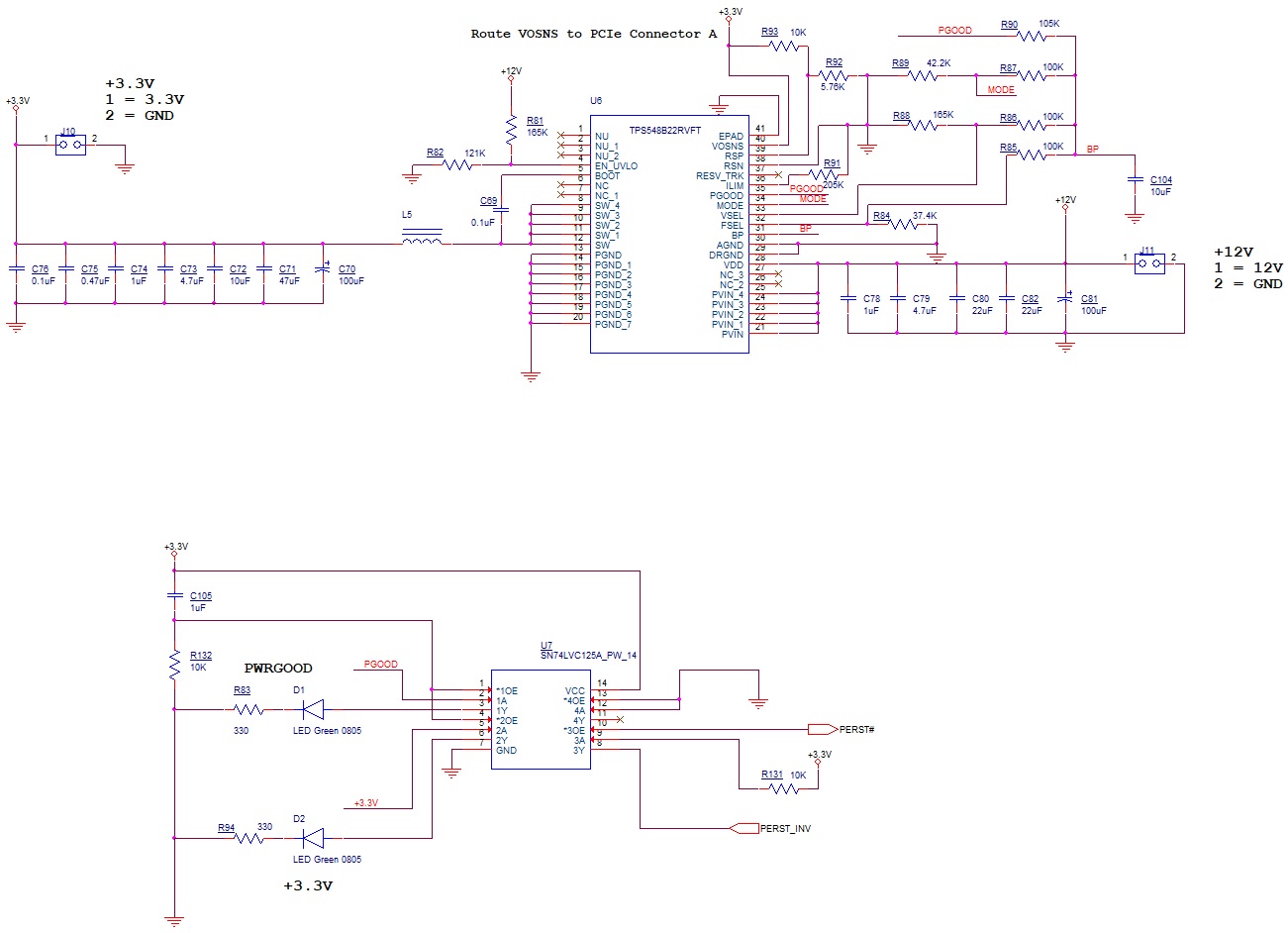 Figure 3-5 Power.
 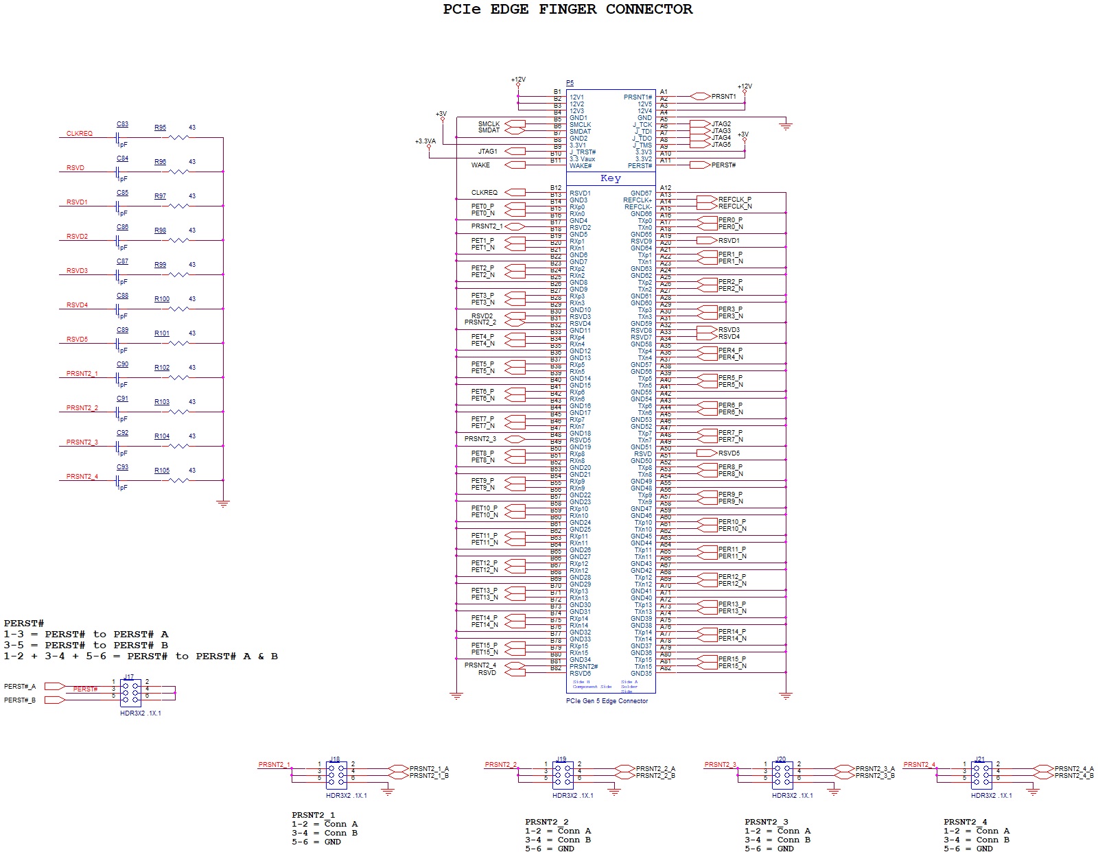 Figure 3-6 EDGE Finger.
 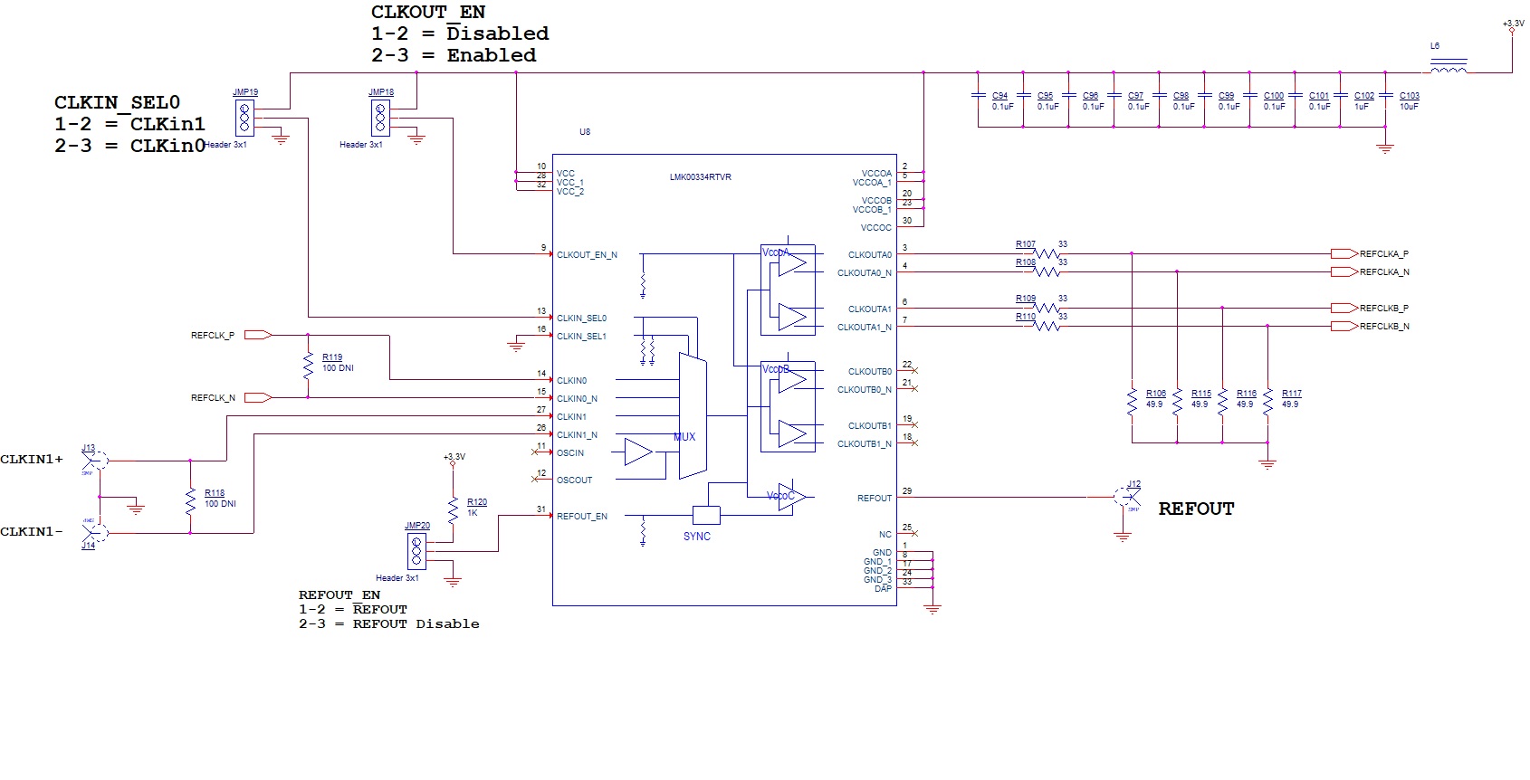 Figure 3-7 PCIe Clock.
 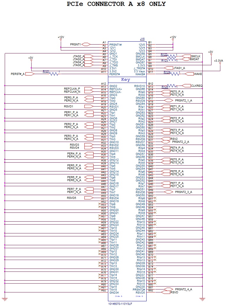 Figure 3-8 PCIe x8 Connector A.
 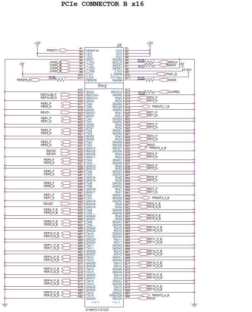 Figure 3-9 PCIe x16 Connector B.