SNVA790A October 2020 – July 2022 LMR36520
4.5 Output Current
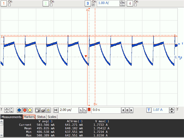
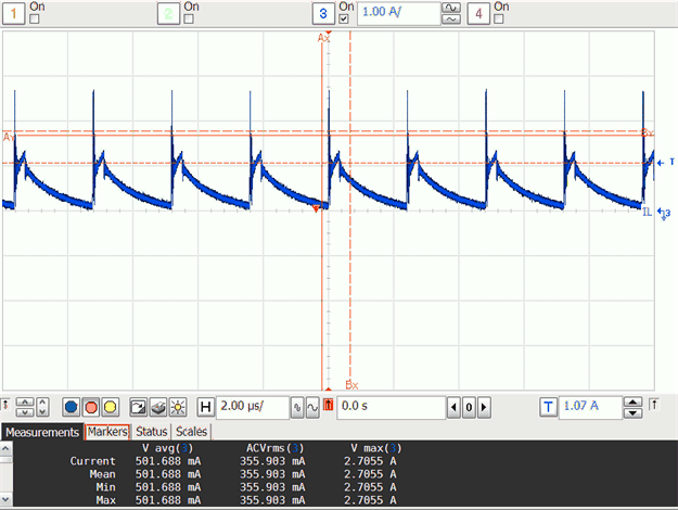
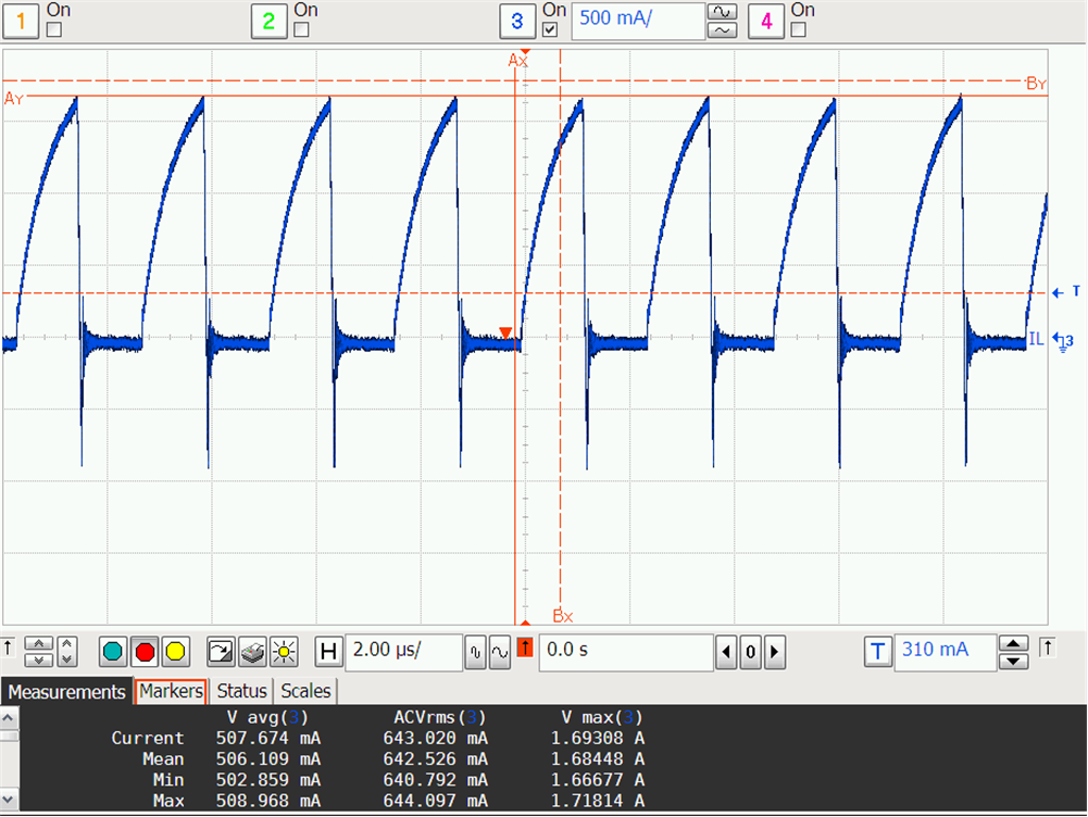
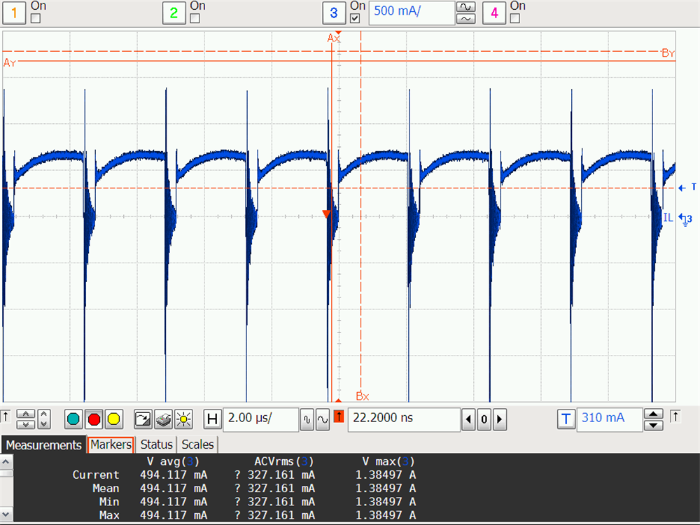
The following output current measurements are shown in more detail to compare with the calculated output capacitor rms currents.
The ACVrms measurement in Figure 4-12 represents the small signal AC component of the primary or secondary winding current waveforms shown. This small signal component is the current that will flow through the output capacitor bank.
 Figure 4-9 Primary winding Current
Measurement at 10 VIN
 Figure 4-10 Primary winding Current
Measurement at 36 VIN
 Figure 4-11 Secondary Winding Current
Measurement at 10 VIN
 Figure 4-12 Secondary Winding Current
Measurement at 36 VIN