SNVA790A October 2020 – July 2022 LMR36520
4.2 Secondary Output Voltage
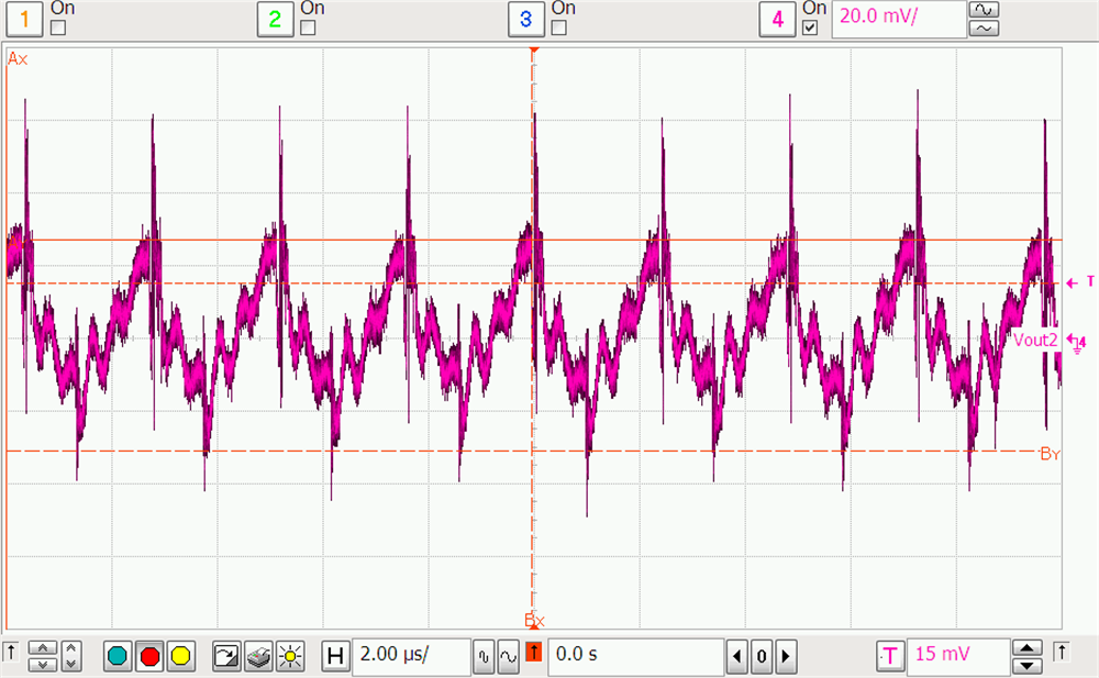
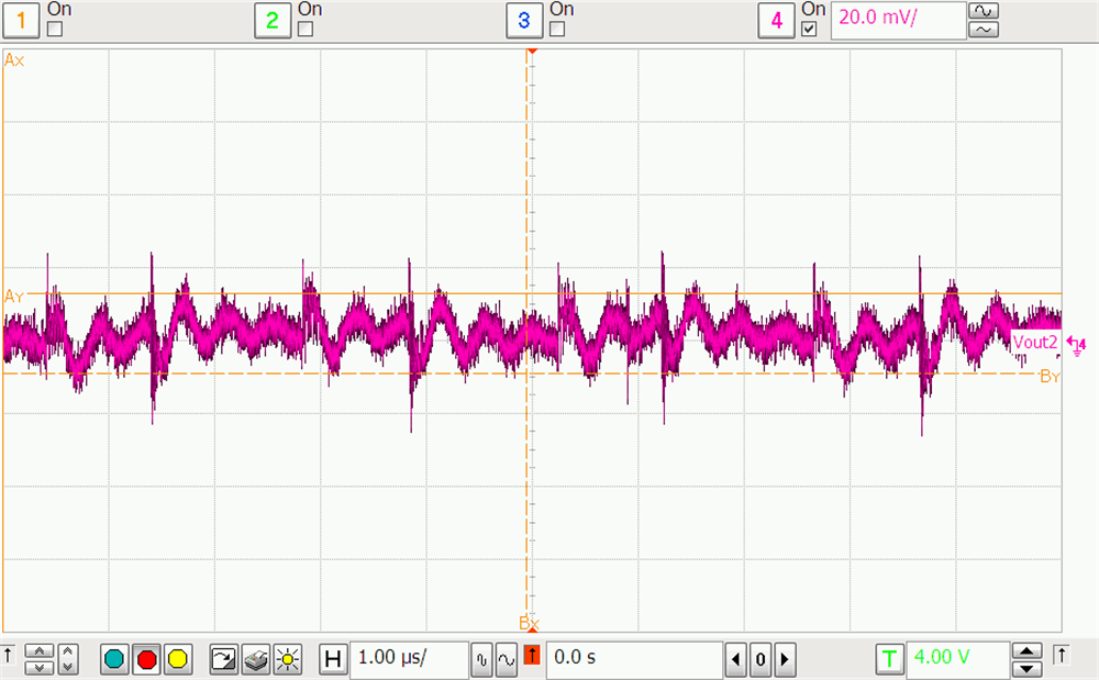
Figure 4-4 and Figure 4-5 show how the secondary output voltage ripple increases from no load on either outputs to full load on both outputs for the same input voltage condition. Although not shown here, the secondary output voltage ripple for the case of 12 VIN, IOUT2 = 500 mA, and IOUT2 = 0 mA is nearly identical to the secondary output voltage ripple waveform shown at full load on both outputs. This represents the worst case of secondary output voltage ripple due to the fact that the secondary output capacitor must supply the entire secondary load current during the device on-time. In contrast, the output voltage ripple is much smaller during the no load condition because the secondary output capacitor only supplies current to the preload resistor.
 Figure 4-4 Secondary Output Voltage
Ripple At Full Load
 Figure 4-5 Secondary Output Voltage
Ripple At No Load