SNVA790A October 2020 – July 2022 LMR36520
4.1 Steady State
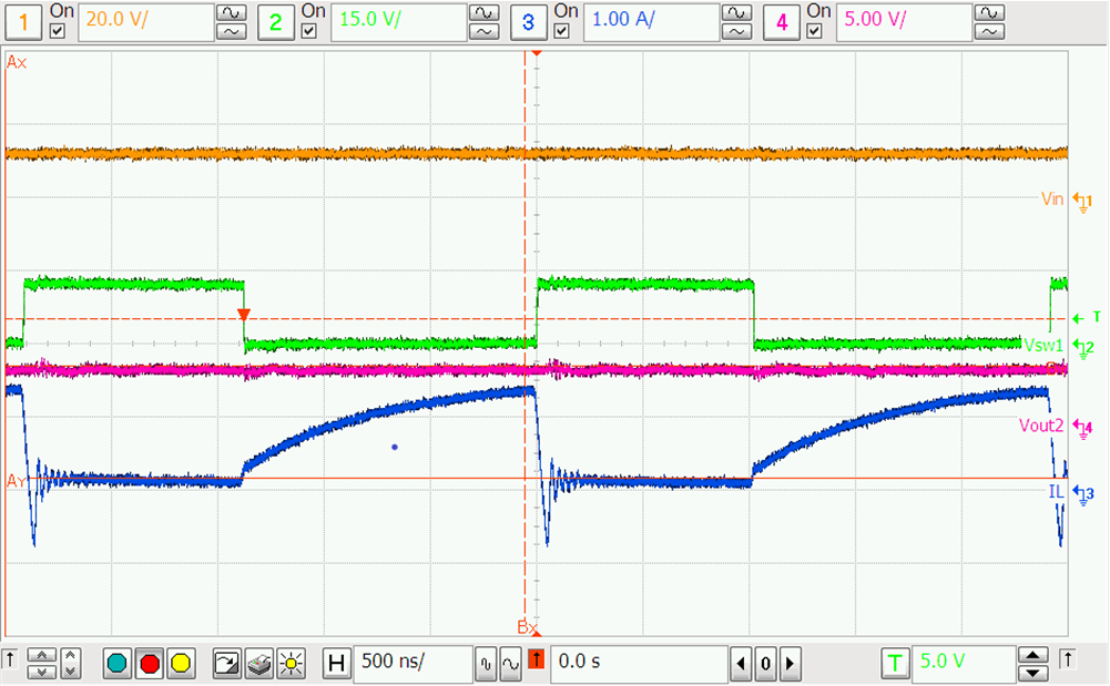
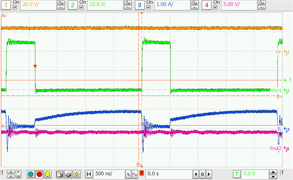
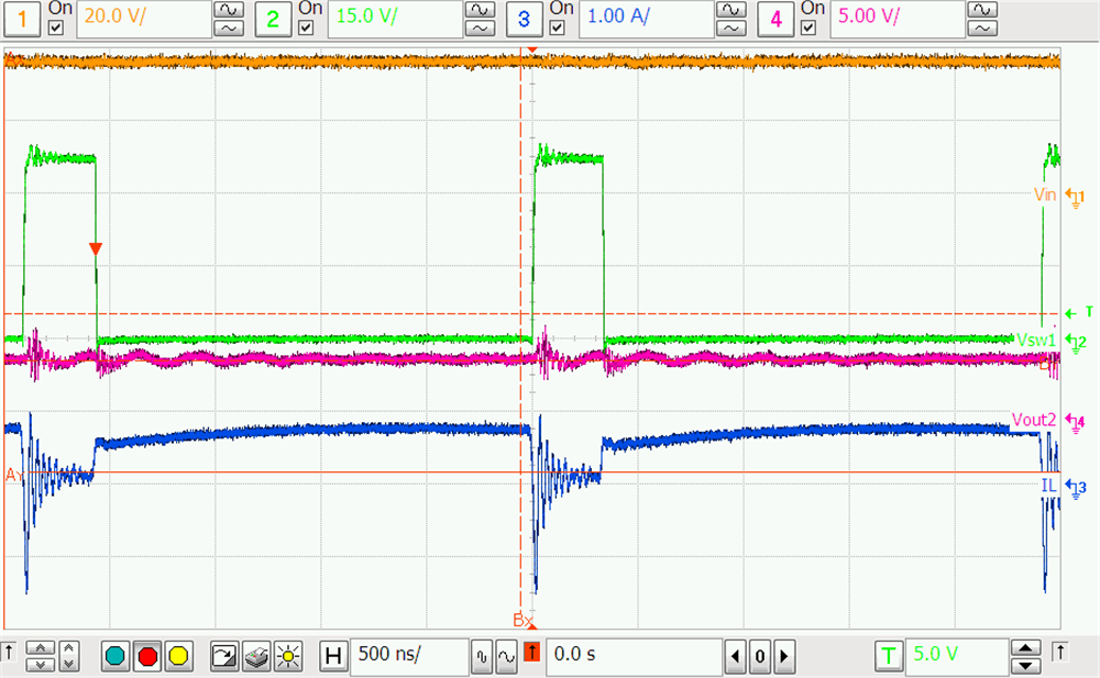
The experimental steady state waveforms shown in Figure 4-1 through Figure 4-3 closely resemble those shown in Figure 2-1. A number of interesting observations can be made through a study of the steady state waveforms. As the input voltage is increased, the ringing seen in the secondary turns current waveform also increases. The secondary output voltage ripple is also proportional to the input voltage. Lastly, the peak current through the secondary turns of the coupled inductor is inversely proportional to the input voltage.
All of the following steady state waveforms show the input voltage VIN, the primary side switch voltage Vsw1, the secondary output voltage Vout2, and the current through the secondary turns of the coupled inductor IL.
 Figure 4-1 12 VIN Full Load
Steady State
 Figure 4-2 24 VIN Full Load
Steady State
 Figure 4-3 36 VIN Full Load
Steady State