SNVA790A October 2020 – July 2022 LMR36520
3 LMR36520 Fly-Buck Converter Design
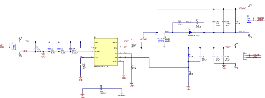
 Figure 3-1 Fly-Buck™
Converter Schematic
Figure 3-1 Fly-Buck™
Converter SchematicTable 3-1 Fly-Buck™ Converter Design Input and Output
Parameters
| VIN minimum | 10 V |
| VIN maximum | 36 V |
| Vout1 | 5 V |
| Iout1 | 500 mA |
| Vout2 | 3.3 V |
| Iout2 | 500 mA |
| Switching frequency | 400 kHz |
In order to operate as a Fly-Buck™ converter, an IC that offers Forced Pulse Width Modulation (FPWM) must be selected to ensure that the part can handle negative inductor current. In this case, the LMR36520FADDA is selected for this reason.
The LMR36520 data sheet should be consulted for recommended values and equations for components such as input capacitor, feedback resistors, EMI filter, feedforward capacitor, CVCC, and bootstrap capacitor. The following design example will focus on calculating component values for Fly-Buck™ converter components specifically.