SNVA967C June 2020 – April 2021 LM34966-Q1 , LM5156 , LM5156-Q1 , LM51561 , LM51561-Q1 , LM51561H , LM51561H-Q1 , LM5156H , LM5156H-Q1
6 Pin Failure Mode Analysis (Pin FMA) – HTSSOP
This section provides a Failure Mode Analysis (FMA) for the pins of the LM5156H, LM5156H-Q1, LM51561H, LM51561H-Q1, and LM34966-Q1 (and HTSSOP package). The failure modes covered in this document include the typical pin-by-pin failure scenarios:
- Pin short-circuited to Ground (see Table 6-2)
- Pin open-circuited (see Table 6-3)
- Pin short-circuited to an adjacent pin (see Table 6-4)
- Pin short-circuited to BIAS supply (see Table 6-5)
Table 6-2 through Table 6-5 also indicate how these pin conditions can affect the device as per the failure effects classification in Table 6-1.
| Class | Failure Effects |
|---|---|
| A | Potential device damage that affects functionality |
| B | No device damage, but loss of functionality |
| C | No device damage, but performance degradation |
| D | No device damage, no impact to functionality or performance |
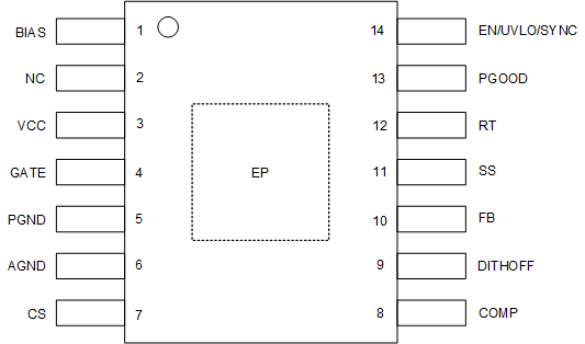
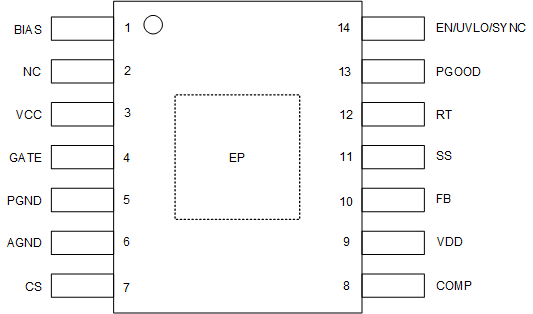
Figure 6-1 shows the LM5156H, LM5156H-Q1, LM51561H, LM51561H-Q1, and LM34966-Q1 (package of HTSSOP) pin diagram. For a detailed description of the device pins please refer to the 'Pin Configuration and Functions' section in the LM5156H, LM5156H-Q1, LM51561H, LM51561H-Q1, and LM34966-Q1 datasheet.
 Figure 6-1 Pin Diagram LM5156H, LM5156H-Q1, LM51561H, LM51561H-Q1
 Figure 6-2 Pin Diagram LM34966-Q1
Following are the assumptions of use and the device configuration assumed for the pin FMA in this section:
- Device used within the Recommended Operating Conditions and the Absolute Maximum Ratings found in the LM5156H, LM5156H-Q1, LM51561H, LM51561H-Q1, and LM34966-Q1 data sheet.
- Configuration as boost converter as shown in the Application and Implementation section found in the LM5156H, LM5156H-Q1, LM51561H, LM51561H-Q1, and LM34966-Q1 data sheet.
| Pin Name | Pin No. | Description of Potential Failure Effect(s) | Failure Effect Class |
|---|---|---|---|
| BIAS | 1 | Device unpowered. Device is not functional. | B |
| NC | 2 | No effect. Normal operation | D |
| VCC | 3 | VCC regulator short circuit. Device shuts down due to VCC undervoltage. VCC regulator may be disabled if thermal shutdown is triggered. | B |
| GATE | 4 | Gate driver not functional. In boost operation, the output voltage is out of regulation. Output voltage is equal to input voltage minus diode forward voltage drop. Potential damage to pin | A |
| PGND | 5 | No effect. Normal operation | D |
| AGND | 6 | No effect. Normal operation | D |
| CS | 7 | Loss of current sense information and loss of current limit. Loop is unstable and there is potential inductor saturation. | B |
| COMP | 8 | Device out of regulation. Device is not switching. | B |
| DITHOFF | 9 | LM5156H, LM5156H-Q1, LM51561H, LM51561H-Q1: Spread Spectrum enabled. | B/D |
| VDD | 9 | LM34966-Q1: Switching frequency may be impacted. | B |
| FB | 10 | Output voltage rises uncontrolled. Potential damage to BIAS pin, if BIAS is connected to VOUT. | A |
| SS | 11 | During soft start, SS pin stuck low. The
device does not start-up. The device stops switching during operation. |
B |
| RT | 12 | Switching frequency is increased to > 2.2 MHz. Device may be unstable. | B |
| PGOOD | 13 | Correct output voltage. Loss of power good functionality | B |
| UVLO/SYNC/EN | 14 | EN stuck low. Device is disabled and in shut down mode. | B |
| Pin Name | Pin No. | Description of Potential Failure Effect(s) | Failure Effect Class |
|---|---|---|---|
| BIAS | 1 | Device unpowered. Device is not functional. | B |
| NC | 2 | No effect. Normal operation | D |
| VCC | 3 | High ripple on VCC pin that may trigger VCC UVLO | B |
| GATE | 4 | Possible device damage | A |
| PGND | 5 | Possible device damage | A |
| AGND | 6 | Possible device damage | A |
| CS | 7 | Loss of current sense information and loss of current limit. Loop is unstable and potential inductor saturation. | B |
| COMP | 8 | Device may be unstable. | C |
| DITHOFF | 9 | LM5156H, LM5156H-Q1, LM51561H, LM51561H-Q1: Spread spectrum in an undefined state | B |
| VDD | 9 | LM34966-Q1: Switching frequency may be impacted. | B |
| FB | 10 | Output voltage rises uncontrolled. Potential damage to BIAS pin if BIAS is connected to VOUT. | A |
| SS | 11 | During soft start, SS pin pulled high.
The device soft start time reduced to 0. High inrush current
possible. No effect during operation. |
C |
| RT | 12 | Internal oscillator not functional. Device stops switching operation. | B |
| PGOOD | 13 | Correct output voltage. Loss of power-good functionality. | C |
| UVLO/SYNC/EN | 14 | State of EN/UVLO/SYNC undetermined. Device may be in shut down or standby mode or enabled. | B |
| Pin Name | Pin No. | Shorted to | Description of Potential Failure Effect(s) | Failure Effect Class |
|---|---|---|---|---|
| BIAS | 1 | NC | No effect. Normal operation | D |
| NC | 2 | VCC | No effect. Normal operation | D |
| VCC | 3 | GATE | Gate driver not functional. Output voltage is out of regulation. Potential damage to pin | A |
| GATE | 4 | GND | Gate driver not functional. Output voltage is out of regulation. In boost operation, the output voltage is equal to input voltage minus diode forward voltage drop. Potential damage to pin | A |
| PGND | 5 | AGND | Normal operation | D |
| AGND | 6 | CS | See Table 6-2. | B |
| CS | 7 | COMP | Not considered. Corner pin | D |
| COMP | 8 | DITHOFF | LM5156H, LM5156H-Q1, LM51561H, LM51561H-Q1: Potential damage to part if current into pin exceeds 1.6 mA. | A |
| DITHOFF | 9 | FB | LM5156H, LM5156H-Q1, LM51561H, LM51561H-Q1: Spread spectrum functionality undeterminded. Output voltage may be out of regulation. | B |
| COMP | 8 | VDD | LM34966-Q1: Potential damage to part if current into pin exceeds 1.6 mA. | A |
| VDD | 9 | FB | LM34966-Q1: FB regulates to 1 V and output voltage may be out of regulation. | B |
| FB | 10 | SS | COMP pin voltage is clamped to 1 V. Device is not switching and out of regulation. | B |
| SS | 11 | RT | Output voltage regulates to VOUT/2. Switching frequency may be incorrect. | B |
| RT | 12 | PGOOD | If FB < 0.9 V (falling) and PGOOD
active low, the switching frequency increased to > 2.2 MHz.
Device may be unstable. If FB > 0.95 V (rising) and PGOOD is pulled up externally, the internal oscillator stops. Potential device damage if pull up voltage is > 3.8 V. |
A |
| PGOOD | 13 | UVLO/SYNC/EN | Potential damage to device if pin 14 is directly connected to supply. | A |
| UVLO/SYNC/EN | 14 | BIAS | Not considered. Corner pin | D |
| Pin Name | Pin No. | Description of Potential Failure Effect(s) | Failure Effect Class |
|---|---|---|---|
| BIAS | 1 | No effect. Normal operation | D |
| NC | 2 | No effect. Normal operation | D |
| VCC | 3 | Potential device damage if BIAS voltage
is greater 18 V. Normal operation if BIAS voltage is below 18 V. |
A/D |
| GATE | 4 | External MOSFET turned on constantly. Potential damage of external component | A |
| PGND | 5 | Device is unpowered. Device is not functional. Observe that the absolute maximum ratings for all pins of the device are met, otherwise device damage may be plausible. | A |
| AGND | 6 | Device is unpowered. Device is not functional. Observe that the absolute maximum ratings for all pins of the device are met, otherwise device damage may be plausible. | A |
| CS | 7 | Potential device damage. Absolute maximum rating for this pin is 0.3 V. | A |
| COMP | 8 | Potential device damage if current into pin exceeds 1.6 mA. | A |
| DITHOFF | 9 | LM5156H, LM5156H-Q1, LM51561H, LM51561H-Q1: Potential device damage if BIAS voltage is greater 18 V | A |
| VDD | 9 | LM34966-Q1: Potential device damage if BIAS voltage is greater 18 V | A |
| FB | 10 | Potential device damage if BIAS voltage is greater 4.0 V | A |
| SS | 11 | Potential device damage if BIAS voltage is greater 3.8 V | A |
| RT | 12 | Potential device damage if BIAS voltage is greater 3.8 V | A |
| PGOOD | 13 | Potential device damage if BIAS voltage is greater 18 V or current into pin exceeds 1 mA | A |
| UVLO/SYNC/EN | 14 | No effect. Normal operation | D |