SNVAA73 may 2023 LM53602 , LM53602-Q1 , LM53603-Q1 , LM63625-Q1 , LM63635-Q1 , LMR14020-Q1 , LMR14030-Q1
6 Converter With Dedicated RBOOT Pin
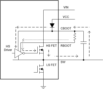
The value of RBOOT depends on the size of the high side MOSFET. For most applications, approximately 5 Ω to 10 Ω is used. If the boot resistor value is too large, the boot capacitor can not fully charge in each cycle. When the value of the boot resistor is too large, the gate driver does not have sufficient voltage to keep the high-side FET on and can turn off in the middle of the cycle. This gate driver behavior limits the amount of ringing that can be reduced with the boot resistor method. To allow optimization of EMI with more flexibility, the LM61440/60 and LM61480/95 families are designed with a dedicated RBOOT pin to allow a resistor to select the strength of the high-side FET driver during turn on. Figure 6-1 shows the integrated RBOOT pin. The current drawn through the RBOOT pin, represented by the dotted loop in Figure 6-1, is magnified and drawn through from CBOOT (the dashed line in Figure 6-1). This feature allows a wide range of RBOOT values to optimize EMI.
 Figure 6-1 Simplified Circuit Showing How
RBOOT Pin Functions