SNVSAA7B December   2015  – July 2021 LM53625-Q1 , LM53635-Q1

PRODUCTION DATA  

  1. Features
  2. Applications
  3. Description
  4. Revision History
  5. Device Comparison
  6. Pin Configuration and Functions
  7. Specifications
    1. 7.1 Absolute Maximum Ratings
    2. 7.2 ESD Ratings
    3. 7.3 Recommended Operating Conditions
    4. 7.4 Thermal Information
    5. 7.5 Electrical Characteristics
    6. 7.6 System Characteristics
    7. 7.7 Timing Characteristics
    8. 7.8 Typical Characteristics
  8. Detailed Description
    1. 8.1 Overview
    2. 8.2 Functional Block Diagram
      1. 8.2.1 Control Scheme
    3. 8.3 Feature Description
      1. 8.3.1 RESET Flag Output
      2. 8.3.2 Enable and Start-Up
      3. 8.3.3 Soft-Start Function
      4. 8.3.4 Current Limit
      5. 8.3.5 Hiccup Mode
      6. 8.3.6 Synchronizing Input
      7. 8.3.7 Undervoltage Lockout (UVLO) and Thermal Shutdown (TSD)
      8. 8.3.8 Input Supply Current
    4. 8.4 Device Functional Modes
      1. 8.4.1 AUTO Mode
      2. 8.4.2 FPWM Mode
      3. 8.4.3 Dropout
      4. 8.4.4 Input Voltage Frequency Foldback
    5. 8.5 Spread-Spectrum Operation
  9. Application and Implementation
    1. 9.1 Application Information
    2. 9.2 Typical Applications
      1. 9.2.1 General Application
        1. 9.2.1.1 Design Requirements
        2. 9.2.1.2 Detailed Design Procedure
          1. 9.2.1.2.1 External Components Selection
            1. 9.2.1.2.1.1 Input Capacitors
              1. 9.2.1.2.1.1.1 Input Capacitor Selection
            2. 9.2.1.2.1.2 Output Inductors and Capacitors Selection
              1. 9.2.1.2.1.2.1 Inductor Selection
              2. 9.2.1.2.1.2.2 Output Capacitor Selection
          2. 9.2.1.2.2 Setting the Output Voltage
            1. 9.2.1.2.2.1 FB for Adjustable Versions
          3. 9.2.1.2.3 VCC
          4. 9.2.1.2.4 BIAS
          5. 9.2.1.2.5 CBOOT
          6. 9.2.1.2.6 Maximum Ambient Temperature
        3. 9.2.1.3 Application Curves
      2. 9.2.2 Fixed 5-V Output for USB-Type Applications
        1. 9.2.2.1 Design Requirements
        2. 9.2.2.2 Detailed Design Procedure
        3. 9.2.2.3 Application Curves
      3. 9.2.3 Fixed 3.3-V Output
        1. 9.2.3.1 Design Requirements
        2. 9.2.3.2 Detailed Design Procedure
        3. 9.2.3.3 Application Curves
      4. 9.2.4 Adjustable Output
        1. 9.2.4.1 Design Requirements
        2. 9.2.4.2 Detailed Design Procedure
        3. 9.2.4.3 Application Curves
    3. 9.3 What to Do and What Not to Do
  10. 10Power Supply Recommendations
  11. 11Layout
    1. 11.1 Layout Guidelines
    2. 11.2 Layout Example
  12. 12Device and Documentation Support
    1. 12.1 Device Support
      1. 12.1.1 Third-Party Products Disclaimer
    2. 12.2 Documentation Support
      1. 12.2.1 Related Documentation
    3. 12.3 Receiving Notification of Documentation Updates
    4. 12.4 Support Resources
    5. 12.5 Trademarks
    6. 12.6 Electrostatic Discharge Caution
    7. 12.7 Glossary
  13. 13Mechanical, Packaging, and Orderable Information

Description

The LM53625-Q1/LM53635-Q1 synchronous buck regulator is optimized for automotive applications, providing an output voltage of 5 V, 3.3 V, or an adjustable output. Advanced high-speed circuitry allows the LM53625-Q1/LM53635-Q1 to regulate from an input of 18 V to an output of 3.3 V at a fixed frequency of 2.1 MHz. Innovative architecture allows this device to regulate a 3.3-V output from an input voltage of only 3.55 V. All aspects of the LM53625-Q1/LM53635-Q1 are optimized for automotive and performance-driven industrial customers. An input voltage range up to 36 V, with transient tolerance up to 42 V, eases input surge protection design. The automotive-qualified Hotrod QFN package with wettable flanks reduces parasitic inductance and resistance while increasing efficiency, minimizing switch node ringing, and dramatically lowering electromagnetic interference (EMI). An open-drain reset output, with built-in filtering and delay, provides a true indication of system status. This feature negates the requirement for an additional supervisory component, saving cost and board space. Seamless transition between PWM and PFM modes and low quiescent current (only 15 µA for the 3.3 V option) ensure high efficiency and superior transient responses at all loads.

Device Information
DEVICE NAME PACKAGE(1) BODY SIZE
LM53625-Q1 VQFN-HR (22) 5.00 mm × 4.00 mm
LM53635-Q1
For all available packages, see the orderable addendum at the end of the data sheet.
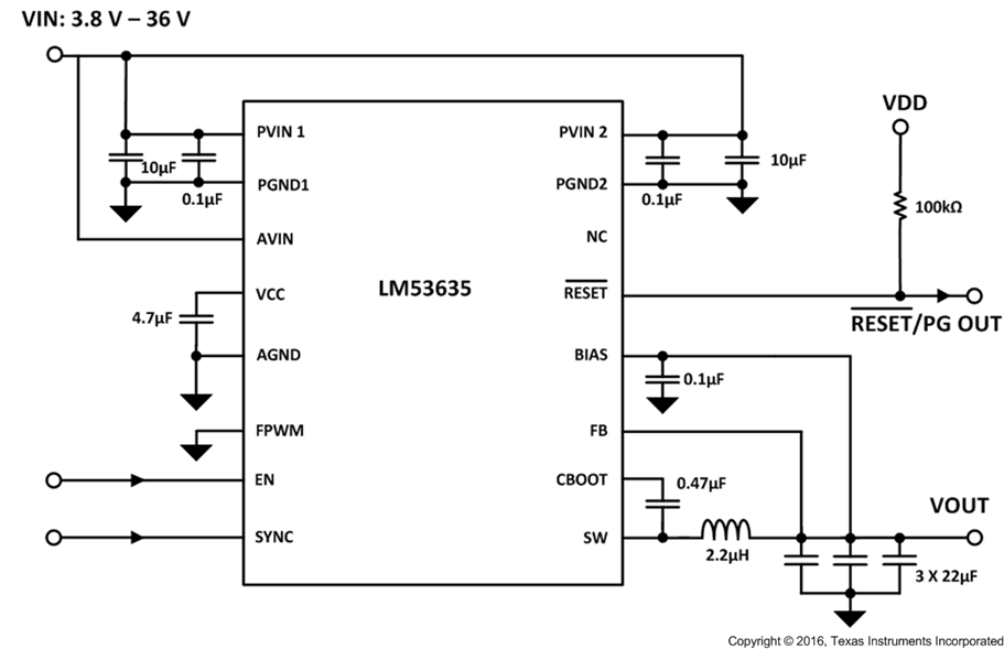
GUID-F7D28089-A1A8-4F22-9203-409FBAD41580-low.pngTypical Application Circuit
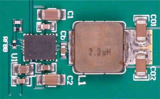
GUID-0C7B6AB8-B819-437B-876D-7EAF4AB75CE0-low.jpgTypical Automotive Layout (22 mm x 12.5 mm)