SNVU770 June 2021 LM5157 , LM5157-Q1 , LM51571-Q1
6.3 Steady-State Waveforms
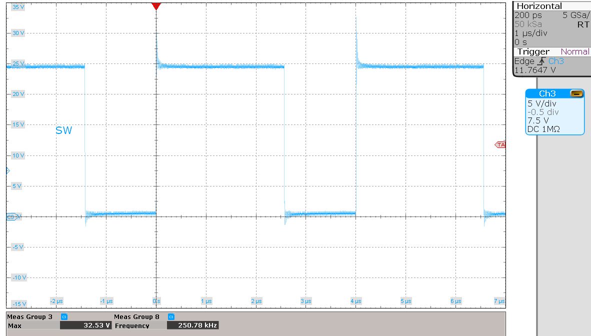 Figure 6-8 SW Waveform at 100% Load,
Under 16-V Maximum VIN
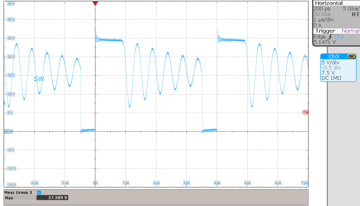 Figure 6-10 SW Waveform at 10% Load,
Under 16-V Maximum VIN
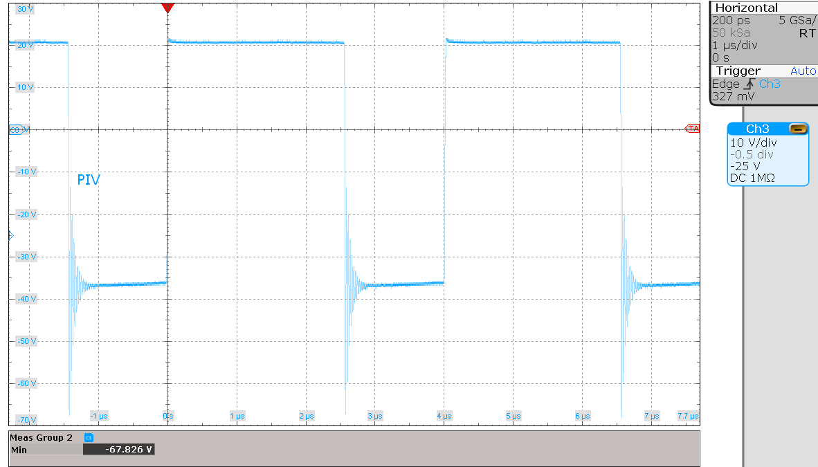 Figure 6-12 PIV of D1 (Vo2 Rectifier)
Under 100% Load and 16-V Maximum VIN
 Figure 6-14 PIV of D5 (Vo3 Rectifier)
Under 100% Load and 16-V Maximum VIN
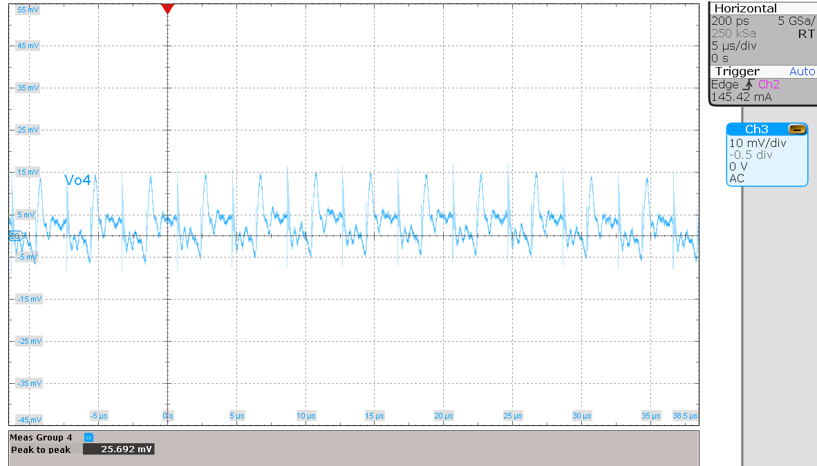 Figure 6-16 Isolated Output Vo4 Ripple
Voltage Under 150-mA Load
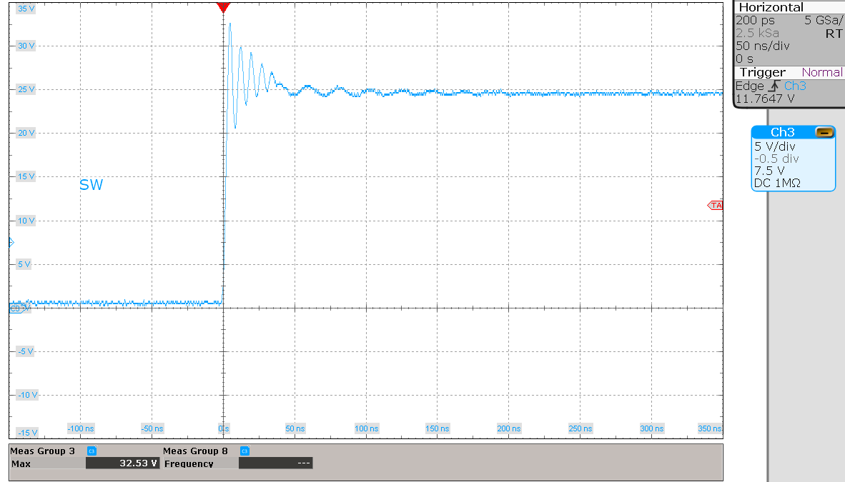 Figure 6-9 Zoomed SW Waveform at 100%
Load, Under 16-V Maximum VIN
 Figure 6-11 PIV of D7 (main Output
Rectifier) Under 100% Load and 16-V Maximum VIN
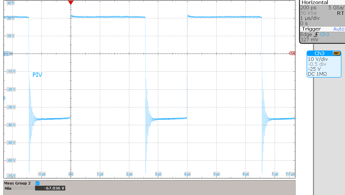 Figure 6-13 PIV of D4 (Vo3 Rectifier)
Under 100% Load and 16-V Maximum VIN
 Figure 6-15 Main Output Vo1 Ripple
Voltage Under 250-mA Load