SPRUI76B March   2017  – June 2022 TMS320F28379D , TMS320F28379D-Q1


  1.   Delfino TMS320F28379D controlCARD R1.3
  2.   Trademarks
  3. 1Introduction
  4. 2Errata
    1. 2.1 Warnings/Notes/Errata
    2. 2.2 Warnings About Specific controlCARD Revisions
  5. 3Getting Familiar With the controlCARD
    1. 3.1 F28379D controlCARD Features
    2. 3.2 Assumed Operating Conditions
    3. 3.3 Using the controlCARD
    4. 3.4 Experimentation Software
  6. 4Special Notes on Connectivity
    1. 4.1 xds100v2 Emulator and SCI/UART Connectivity
    2. 4.2 External Connector – J9
    3. 4.3 Evaluation of the Analog-to-Digital Converters (ADCs)
  7. 5Hardware References
  8. 6References
  9. 7Revision History

Hardware References

Table 5-1 shows the various connections available on the board. Figure 5-1 illustrates the location of many of these components on the board.

WARNING:

When the controlCARD is used in a high-voltage setup, it is the user’s responsibility to confirm that the voltages and isolation requirements are identified and understood prior to energizing the board or simulation. When energized, the controlCARD or components connected to the controlCARD should not be touched. Furthermore, the capacitor A:C31 should be removed to minimize the possibility of leakage current flowing across the isolation barrier of the controlCARD.
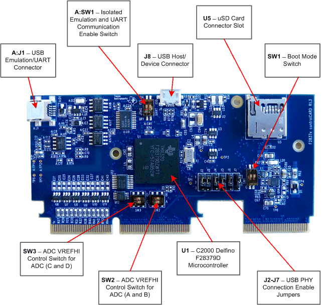
GUID-4A7370F8-35B2-42CC-9C3C-8812DEE7F372-low.gifFigure 5-1 Key components on the controlCARD
Table 5-1 Hardware References
Connectors
A:J1 Emulation/UART connector - USB mini A connector used to provide xds100v2 emulation and USB-to-UART(SCI) communication through FTDI logic. A:SW1 determines which connections are enabled to the MCU.
U5 SD Micro card slot – connects to MCU via SPI
J8 USB connector – USB micro AB connector supports USB 2.0 host/device
J9 Enables a secondary board to have access to the F28379D’s EMIF2 and several other digital signals.
Jumpers
J2-J7 USB PHY connection enable/disable jumpers:
  • All jumpers up – The MCU will be connected to the USB PHY on the controlCARD via GPIOs 42, 43, 46, 47, 120, and 121
  • .All jumpers down – The MCU will not connect to the USB PHY and all signals will instead go through the 180-pin controlCARD connector.
LEDs
LD1 Turns on when the controlCARD is powered ON (green)
LD2 Controlled by GPIO-31 with negative logic (red)
LD3 Controlled by GPIO-34 with negative logic (red)
A:D2 Turns on when ISO JTAG logic is powered on (green)
A:D3 JTAG/UART RX toggle indicator (blue)
A:D4 JTAG/UART TX toggle indicator (blue)
Resistors and Capacitors
R59, R60 Alternate Reference Configuration Resistors
These resistors allow the user to choose whether the alternate reference for the ADCs will be given by:
  • If R59 is unpopulated & R60 is populated
    A precision 3.0V reference (REF5030)
  • If R59 is populated & R60 is unpopulated
    The reference will be given by pin 45 of the HSEC controlCARD connector. This will presumably allow the baseboard to provide the desired voltage reference.
R27-R50 and C18-C41 Optional RC input filter for all ADC inputs
Switches (default position in BOLD)
SW1 Boot Mode Switch:
Controls the Boot Options of the F28379D device. For more information. (0 is down, 1 is up), see the device-specific data sheet.
Mode # Switch Position 1 (GPIO-72) Switch Position 2 (GPIO-84) Boot from 00 0 0 Parallel I/O 01 0 1 Boot from SCI 02 1 0 Wait Boot Mode 03 1 1 Get Mode (Flash by default)
Mode # Switch Position 1
(GPIO-72)
Switch Position 2
(GPIO-84)
Boot from
00 0 0 Parallel I/O
01 0 1 Boot from SCI
02 1 0 Wait Boot Mode
03 1 1 Get Mode (Flash by default)
SW2 ADC VREFHI Control Switch for ADC modules A & B:
Switch 1 (lower switch) – VREFHI Control Switch for ADC module A:
  • In the left position – ADC-A is configured to use VDDA (3.3 V) as the ADC’s voltage reference. The full-scale range of this ADC will be 0-3.3 V, but the ADC will have reduced accuracy/precision.
  • In the right position – ADC-A is configured to either use a precise 3.0 V voltage reference or an external voltage may be used as a reference. R59 and R60 determine which setting is used (see description for R59/R60, above)
Switch 2 (upper switch) – VREFHI Control Switch for ADC module B:
  • In the left position – ADC-B is configured to use VDDA (3.3 V) as the ADC’s voltage reference. The full-scale range of this ADC will be 0-3.3 V, but the ADC will have reduced accuracy/precision.
  • In the right position – ADC-B is configured to either use a precise 3.0 V voltage reference or an external voltage may be used as a reference. R59 and R60 determine which setting is used (see description for R59/R60, above)
SW3 ADC VREFHI Control Switch for ADC modules C & D:
Switch 1 (lower switch) – VREFHI Control Switch for ADC module C:
  • In the left position – ADC-C is configured to use VDDA (3.3 V) as the ADC’s voltage reference. The full-scale range of this ADC will be 0-3.3V, but the ADC will have reduced accuracy/precision.
  • In the right position – ADC-C is configured to either use a precise 3.0 V voltage reference or an external voltage may be used as a reference. R59 and R60 determine which setting is used (see description for R59/R60, above)
Switch 2 (upper switch) – VREFHI Control Switch for ADC module D:
  • In the left position – ADC-D is configured to use VDDA (3.3 V) as the ADC’s voltage reference. The full-scale range of this ADC will be 0-3.3V, but the ADC will have reduced accuracy/precision.
  • In the right position– ADC-D is configured to either use a precise 3.0 V voltage reference or an external voltage may be used as a reference. R59 and R60 determine which setting is used (see description for R59/R60, above).
A:SW1 Isolated emulation and UART communication enable switches:
Switch Position 1 – JTAG Enable:
  • ON – All signals between the xds100v2 emulation logic and the MCU will be connected. This setting is valid when the MCU is being debugged or programmed via the on-card xds100v2 emulator.
  • OFF – The xds100v2 emulation logic will NOT be connected to the MCU. This setting is valid when the device will boot from FLASH, boot from a peripheral directly, or when an external JTAG emulator will be used.
Switch Position 2 – ISO UART communication enable:
  • ON – The C2000 MCU’s GPIO-28 (and pin 76 of the 180-pin controlCARD connector) will be coupled to the FTDI’s USB-to-Serial adapter. This allows UART communication to a computer via the FTDI chip. However, in this position, GPIO-28 will be forced high by the FTDI chip. Functionality of pin 76 of the connector will be limited.
  • OFF – The C2000 MCU will NOT be connected to the FTDI USB-to-Serial adapter. Pin 76 of the 180-pin controlCARD connector will be directly connected to GPIO-28.