SPRUIU8A March 2020 – August 2021 TMS320F280040-Q1 , TMS320F280040C-Q1 , TMS320F280041 , TMS320F280041-Q1 , TMS320F280041C , TMS320F280041C-Q1 , TMS320F280045 , TMS320F280048-Q1 , TMS320F280048C-Q1 , TMS320F280049 , TMS320F280049-Q1 , TMS320F280049C , TMS320F280049C-Q1
6.2 Programming Static Code – Loading via Code Composer Studio (CCS)
The hardware used in the illustrated steps is an F28004x ControlCARD on a ControlCARD docking station Rev4.1. If a JTAG connection is available, then CCS can be used to load Flash banks 0 and 1 with static code. Note:
Make sure you have the settings in CCS (or your target configuration file – by right clicking and selecting properties) as shown in Figure 6-1 before loading the images. Build the flashapi_ex2_sci_kernel project in both BANK0_LDFU and BANK1_LDFU configurations, and load each to target. The CCS flash plugin will load the contents on to flash.
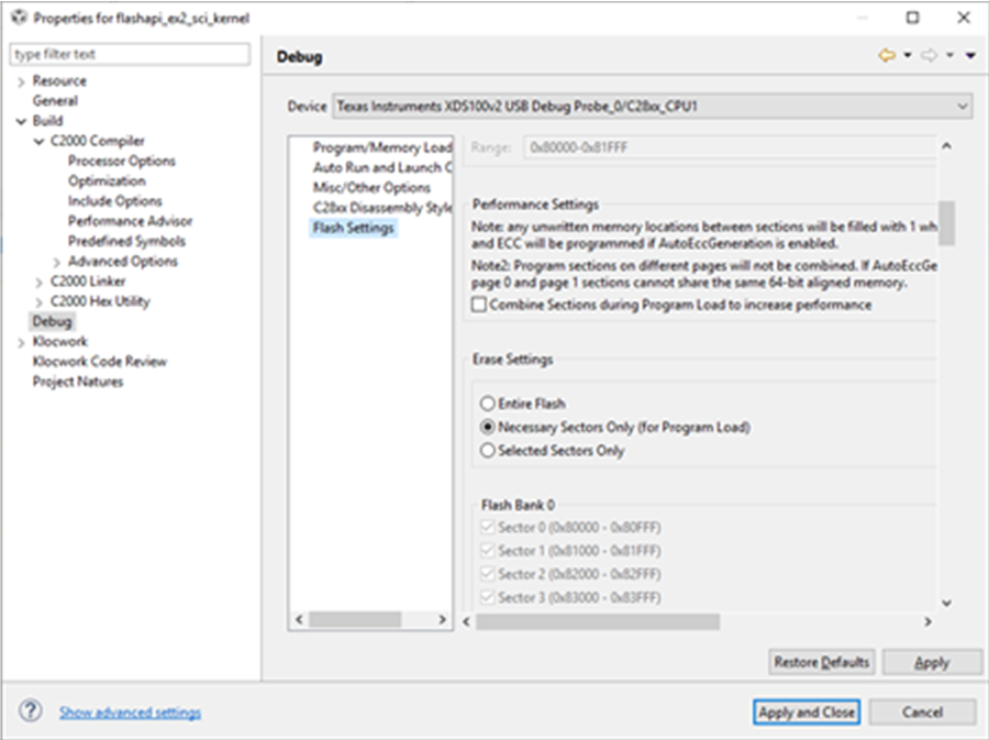 Figure 6-1 Flash Settings to Only Erase Necessary Sectors
- Load BANK0 static image (BANK0_LDFU of flashapi_ex2_sci_kernel project).
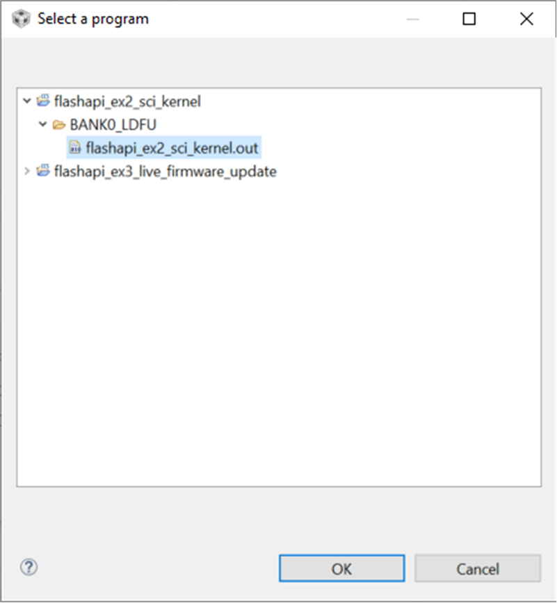 Figure 6-2 Selecting Kernel to Load to Flash Bank 0
After the static contents are loaded on BANK0, the first thing that happens is the execution of the bank selection logic that will determine that application firmware is not programmed in either bank.
Control will pass to the flash kernel, which will be ready to program the application in BANK1. The CCS view will look Figure 6-3 (the program will not stop at main(), but will be running, awaiting a SCI command):
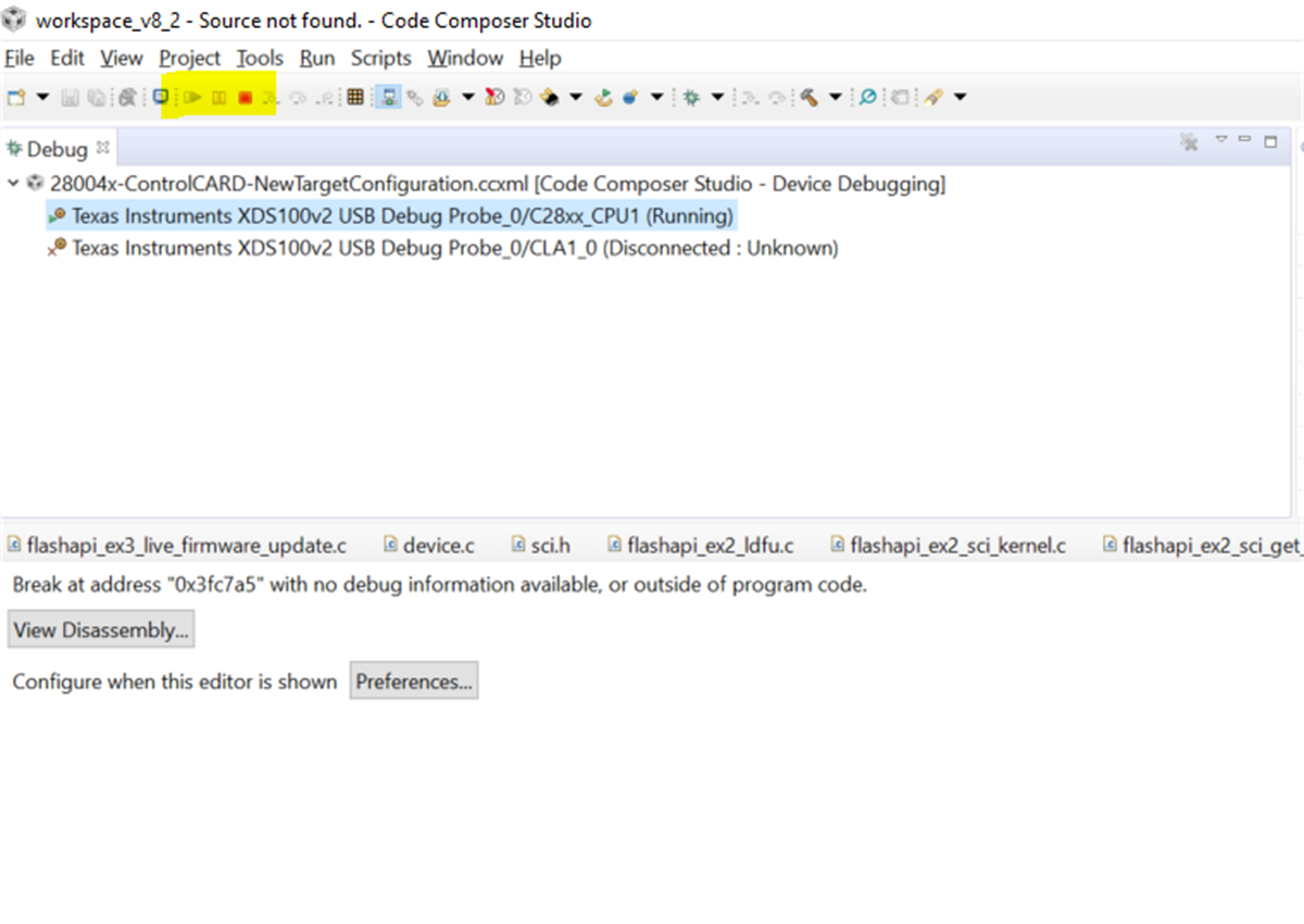 Figure 6-3 CCS Window view After Programming Bank 0 Flash Kernel
 - Verify the Kernel content of BANK0 by opening the Memory Browser window in CCS, and entering address 0x80000.
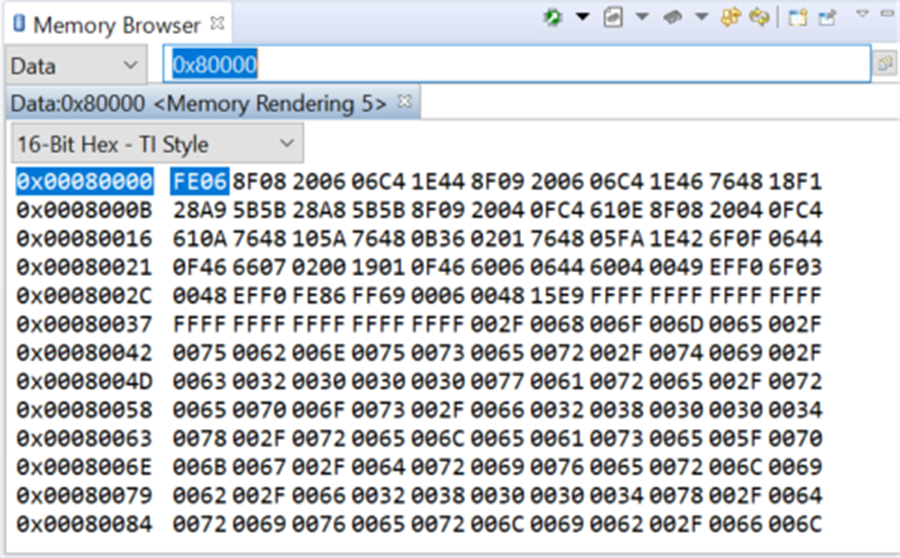 Figure 6-4 CCS Memory Browser View to Verify Successful Kernel Programming of Bank 0
 - Now switch to the Windows command prompt, and execute the command below: serial_flash_programmer_appln.exe -d f28004x -k f28004x_fw_upgrade_example\flashapi_ex2_sci_kernel.txt -a flashapi_ex3_live_firmware_updateBANK1FLASH.txt -b 9600 -p COMx where x = COM port corresponding to the JTAG connection between the PC and the target board. The COM port number can be found by looking up Ports in Device Manager. This will be populated by virtue of the fact that there is a USB cable connected between the target and the computer, which provides both JTAG and SCI functionality. The example uses a baud rate of 9600. flashapi_ex3_live_firmware_updateBANK1FLASH.txt is generated by building the CCS project flashapi_ex3_live_firmware_update in build configuration BANK1_FLASH.
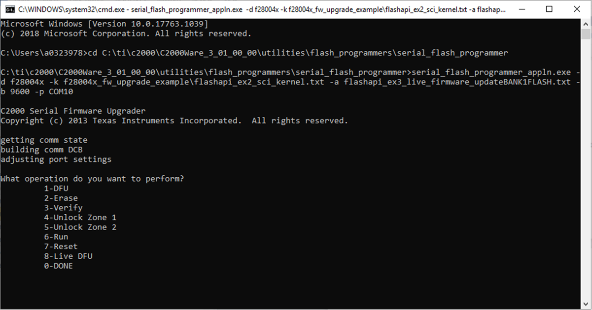 Figure 6-5 LFU Serial Command Invoked From Windows Command Prompt
 - Once LDFU (8) command is selected, the kernel will receive and program the application in BANK1. The application size is about 36KB. Download time will be about 30 seconds.
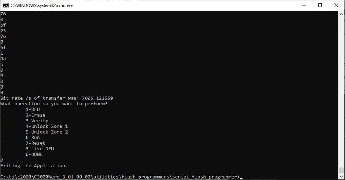 Figure 6-6 Successful Completion of LFU Command to Program Flash Bank 1
 - After transfer is complete, enter 0 to indicate end of command operations. Verify the Application content of BANK1 by opening the Memory Browser window in CCS, and entering address 0x92000.
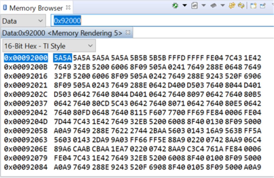 Figure 6-7 CCS Memory Browser View to Verify Successful Programming of Application on Bank 1
The kernel will also update the KEY and revision number in BANK1 sector 2. Now the static image, in programmed BANK0 and application image, is programmed in BANK1.
- At this point, the user can reset the board to see LED2 start blinking.
- Next load BANK1 static image (BANK1_LDFU of flashapi_ex2_sci_kernel project).
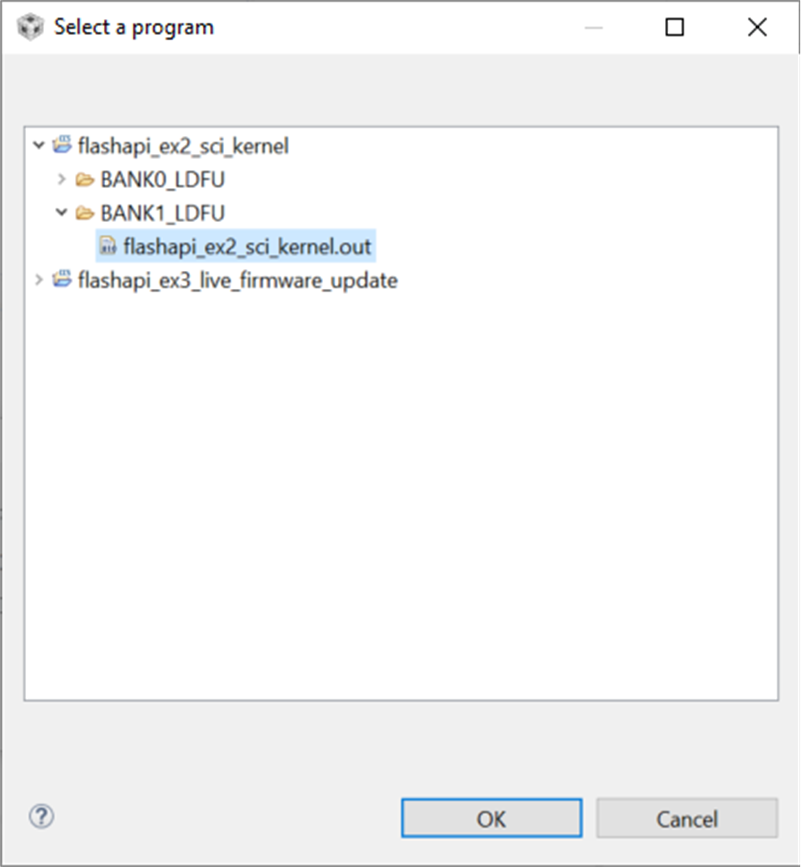 Figure 6-8 Selecting Kernel to Load to Flash Bank 1
 - Verify the Kernel content of BANK1 by opening the Memory Browser window in CCS, and entering address 0x90000.
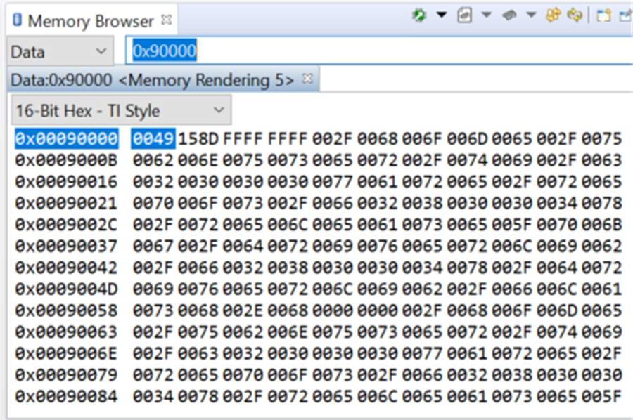 Figure 6-9 CCS Memory Browser View to Verify Successful Kernel Programming of Bank 1
After the static contents are loaded on to BANK1, execution stops at main(). This occurs for the kernel on Bank1 because bank selection logic resides only on Bank0, not on Bank1. Thus, for Bank1, execution flow follows the conventional flow of codestart leading up to main().
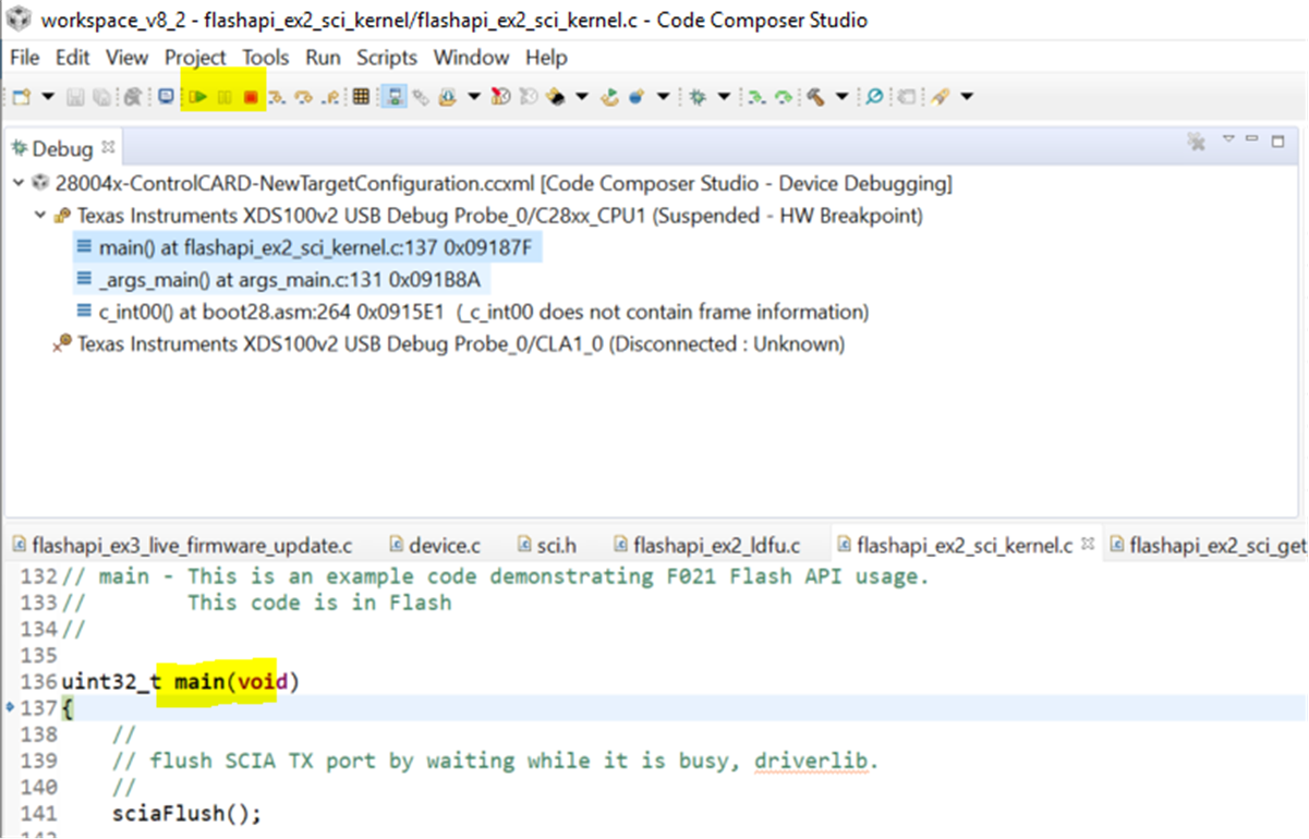 Figure 6-10 CCS Window View After Programming Bank 1 Flash Kernel
 - Press Run in CCS, the bank selection logic will run and execute application from BANK1. Then, execute the below command from command line in PC.
serial_flash_programmer_appln.exe -d f28004x -k f28004x_fw_upgrade_example\flashapi_ex2_sci_kernel.txt -a flashapi_ex3_live_firmware_updateBANK0FLASH.txt -b 9600 -p COMx where x = COM port corresponding to the JTAG connection between the PC and the target board. flashapi_ex3_live_firmware_updateBANK0FLASH.txt is generated by building the CCS project flashapi_ex3_live_firmware_update in build configuration BANK0_FLASH.
 Figure 6-11 LFU Serial Command Invoked From Windows Command Prompt
 - Control will pass to flash kernel from the application and, once LDFU (8) command is selected, the kernel will receive and program the application in BANK0.
- After transfer is complete, enter 0 to indicate end of command operations.
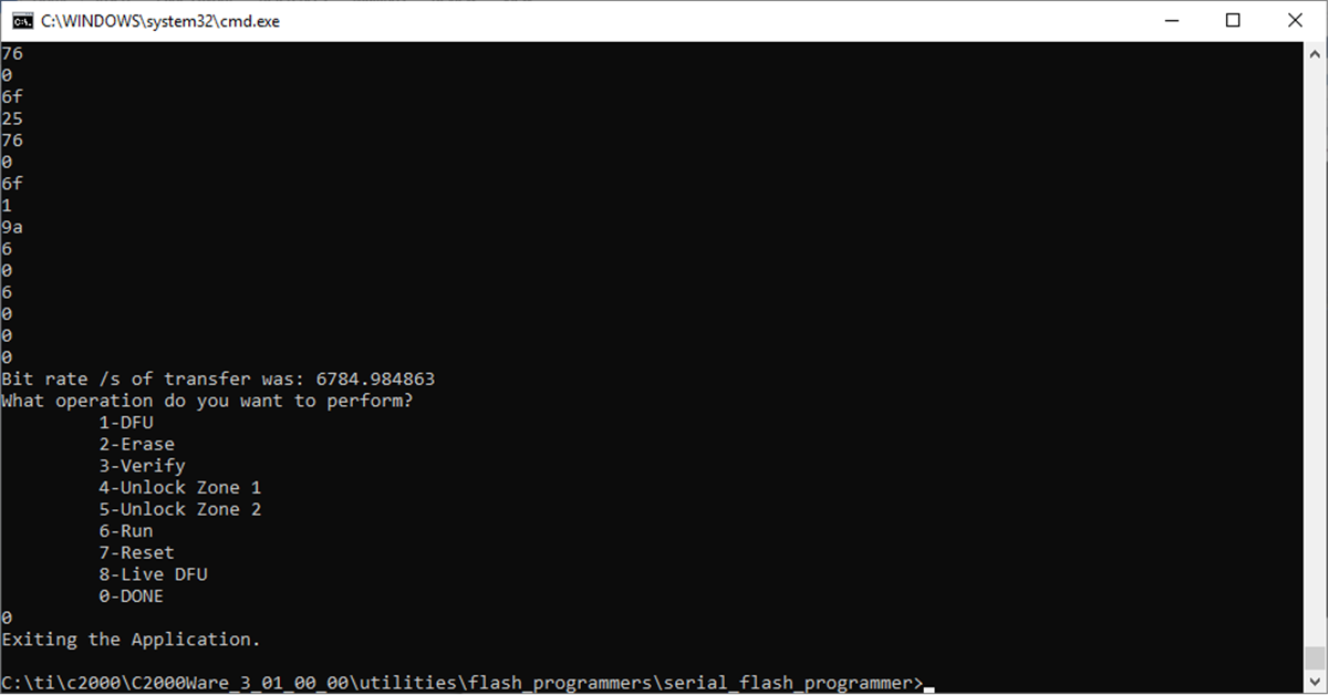 Figure 6-12 Successful Completion of LFU Command to Program Flash Bank 0
The kernel will also update the KEY and revision number in BANK0 sector 2. Now the static image in programmed BANK1 and application image is programmed in BANK0.
- At this point, as before, the user can reset the board, to see LED1 start blinking.