SPRUIU8A March 2020 – August 2021 TMS320F280040-Q1 , TMS320F280040C-Q1 , TMS320F280041 , TMS320F280041-Q1 , TMS320F280041C , TMS320F280041C-Q1 , TMS320F280045 , TMS320F280048-Q1 , TMS320F280048C-Q1 , TMS320F280049 , TMS320F280049-Q1 , TMS320F280049C , TMS320F280049C-Q1
6.3 Live Firmware Update of Application
After programming the static contents, disconnect the debugger and set the boot mode switches to flash boot mode. When the device boots up, it will jump to Flash. The default flash entry point is 0x80000, which is where the static code (Bank selection logic + SCI Flash Kernel) has been programmed in Bank0. The bank selection logic will execute and determine that valid images exist in both Banks 0 and 1 (based on KEY and revision number). Bank0 will be selected to run because, in Section 6.1, it was programmed later so it will be deemed the newest version based on the REV field. So the application firmware in Bank0 will be executed.
The application blinks LED1 at every 1 second. At the same time the application also monitors the serial port to check if it is getting any image for live firmware update.
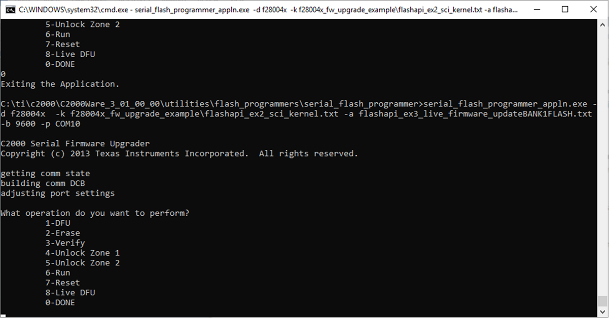
To perform live firmware updates, build the updated application for BANK1 configuration and execute the command shown in Figure 6-13 from the host PC in the command line. Enter ‘8’ for LDFU when the menu is listed. serial_flash_programmer_appln.exe -d f28004x -k f28004x_fw_upgrade_example\flashapi_ex2_sci_kernel.txt -a flashapi_ex3_live_firmware_updateBANK1FLASH.txt -b 9600 -p COMx.
 Figure 6-13 LFU Serial Command Invoked From Windows Command Prompt
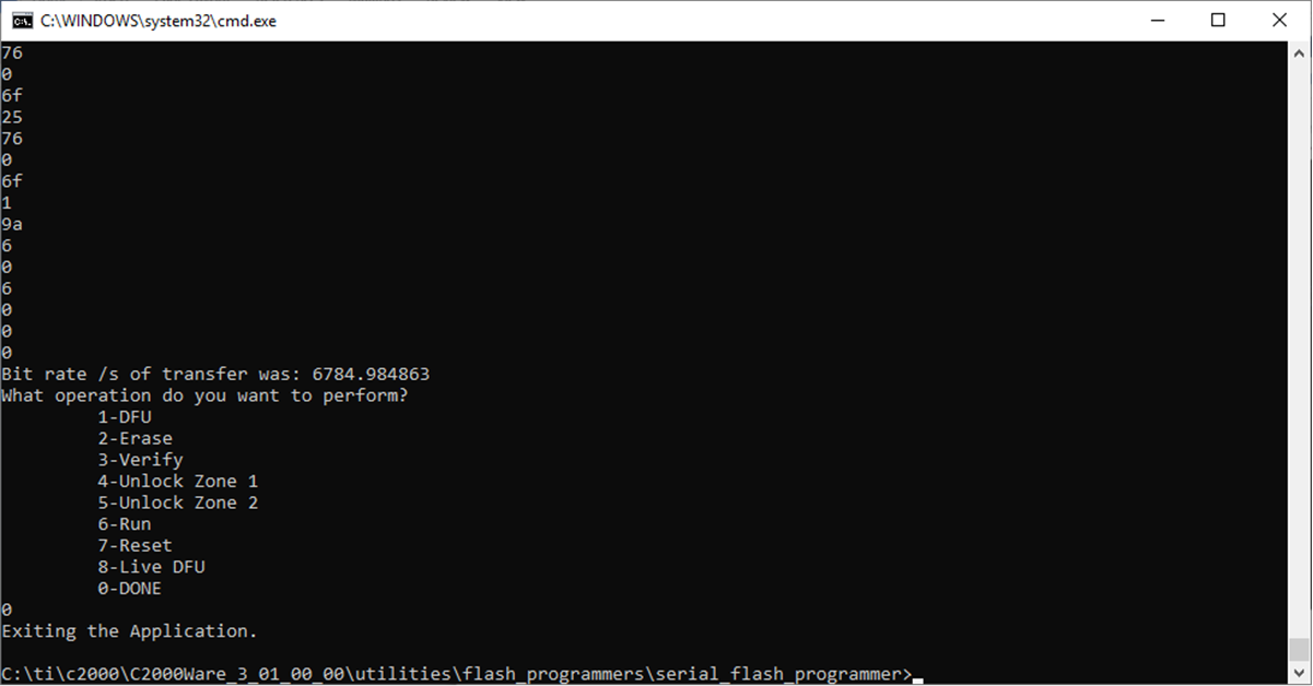
If it receives an image, control will jump to the flash kernel in Bank0 and update the firmware image on Bank1. After transfer is complete, enter 0 to indicate end of command operations. When the new image is being downloaded to Bank1, the application continues to run on Bank0 (LED1 continues to blink at the usual 1s rate). This is because LFU processing occurs in a background loop, not the SCI Receive interrupt. This allows other interrupts, such as the CPU Timer interrupt that toggles the LEDs, to be serviced.
 Figure 6-14 Successful completion of LFU Command to Program Flash Bank
After the Watchdog timer resets, the device resets, and control is passed to the newest application image in Bank1, and LED2 will start blinking.
The manual device reset is no longer required.
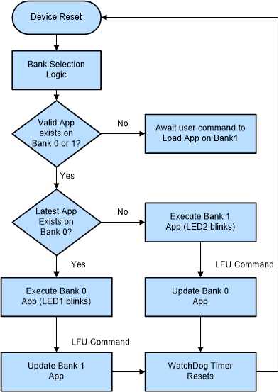
This process can be repeated to update the image in alternate banks. Figure 6-15 illustrates the flow described above.
 Figure 6-15 LFU Code Flow Diagram