SPRUIY9B May 2021 – October 2023
- 1
- Abstract
- Trademarks
- 1Key Features
- 2EVM Revisions and Assembly Variants
- 3Important Usage Notes
-
4System Description
- 4.1 Key Features
- 4.2 Functional Block Diagram
- 4.3 Power-On/Off Procedures
- 4.4
Peripheral and Major Component
Description
- 4.4.1 Clocking
- 4.4.2 Reset
- 4.4.3 Power
- 4.4.4 Configuration
- 4.4.5 JTAG
- 4.4.6 Test Automation
- 4.4.7 UART Interface
- 4.4.8 Memory Interfaces
- 4.4.9 Ethernet Interface
- 4.4.10 USB 3.0 Interface
- 4.4.11 PRU Connector
- 4.4.12 User Expansion Connector
- 4.4.13 MCU Connector
- 4.4.14 Interrupt
- 4.4.15 I2C Interface
- 4.4.16 IO Expander (GPIOs)
-
5Known Issues
- 5.1 Issue 1: LP8733x Max output Capacitance Spec Exceeded on LDO0 and LDO1
- 5.2 Issue 2: LP8733x Output Voltage of 0.9V Exceeds AM64x VDDR_CORE max Voltage Spec of 0.895 V
- 5.3 Issue 3 - SDIO Devices on MMC0 Require Careful Trace Lengths to Meet Interface Timing Requirements
- 5.4 Issue 4 - LPDDR4 Data Rate Limitation in Stressful Conditions
- 5.5 Issue 5 - Junk Character
- 5.6 Issue 6 - Test Power Down Signal Floating
- 5.7 Issue 7 - uSD Boot Not Working
- 6Regulatory Compliance
- 7Revision History
4.4.7 UART Interface
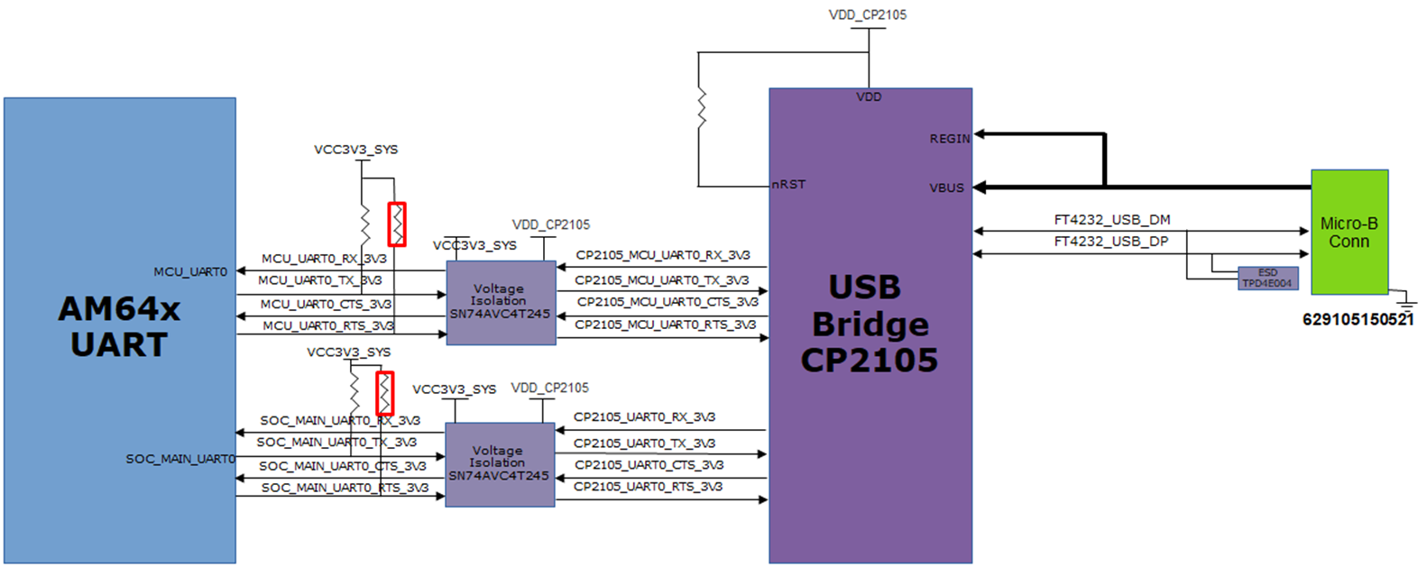
The two UART ports MAIN_UART0 and MCU_UART0 provided by AM64x are connected to two channel USB to UART Bridge (CP2105) and terminated to a USB Micro B Connector J11. Two ports of the CP2105, connected to MAIN_UART0 and MCU_UART0 with the RXD, TXD, RTS and CTS signals.
The USB interface circuit is used in bus powered configuration and a voltage translator (SN74AVC4T245) is used to isolate AM64x IOs. The CP2105 includes an on-chip 5 to 3.45 V voltage regulator. This allows the CP2105 to be configured as a USB bus-powered device. The voltage regulator output appears on the VDD pin and can be used to drive the IO supply as well as one of the supply rails of voltage Translator. Internally the same VDD is used to operate the core section of CP2105. CP2105 also includes an integrated clock and hence no external crystal is required. MAIN_UART0 and MCU_UART0 from SOC are at 3.3V IO level. The devices uses the internal POR Circuit. For normal Operation, the nRST pin needs to be pulled up to 3V3 Supply via 10K Resistor. Since the Device operates in Bus Powered Configuration, VBUS from the USB Connector needs to be connected to “REGIN” pin of CP2105 to serve as the input for the internal regulator.
A ESD protection is provided on USB signals to steer ESD current pulses to VCC or GND. TPD4E004 protects against ESD pulses up to ±15-kV Human-Body Model (HBM) as specified in IEC 61000-4-2 and provides ±8-kV contact discharge and ±12- kV air-gap Discharge. Figure 4-13 shows the dual UART to USB bridge connection with AM64x.
 Figure 4-13 UART Interface