SPRUIY9B May 2021 – October 2023
- 1
- Abstract
- Trademarks
- 1Key Features
- 2EVM Revisions and Assembly Variants
- 3Important Usage Notes
-
4System Description
- 4.1 Key Features
- 4.2 Functional Block Diagram
- 4.3 Power-On/Off Procedures
- 4.4
Peripheral and Major Component
Description
- 4.4.1 Clocking
- 4.4.2 Reset
- 4.4.3 Power
- 4.4.4 Configuration
- 4.4.5 JTAG
- 4.4.6 Test Automation
- 4.4.7 UART Interface
- 4.4.8 Memory Interfaces
- 4.4.9 Ethernet Interface
- 4.4.10 USB 3.0 Interface
- 4.4.11 PRU Connector
- 4.4.12 User Expansion Connector
- 4.4.13 MCU Connector
- 4.4.14 Interrupt
- 4.4.15 I2C Interface
- 4.4.16 IO Expander (GPIOs)
-
5Known Issues
- 5.1 Issue 1: LP8733x Max output Capacitance Spec Exceeded on LDO0 and LDO1
- 5.2 Issue 2: LP8733x Output Voltage of 0.9V Exceeds AM64x VDDR_CORE max Voltage Spec of 0.895 V
- 5.3 Issue 3 - SDIO Devices on MMC0 Require Careful Trace Lengths to Meet Interface Timing Requirements
- 5.4 Issue 4 - LPDDR4 Data Rate Limitation in Stressful Conditions
- 5.5 Issue 5 - Junk Character
- 5.6 Issue 6 - Test Power Down Signal Floating
- 5.7 Issue 7 - uSD Boot Not Working
- 6Regulatory Compliance
- 7Revision History
4.4.2 Reset
The AM64x SoC has the following resets:
- RESETSTATz is the warm reset status output for Main domain.
- PORz_OUT is the power ON reset status output from Main and MCU domain.
- MCU_PORz is the power ON/ Cold Reset input for MCU and Main domain.
- MCU_RESETz is the warm reset input for MCU domain.
- MCU_RESETSTATz is the Warm Reset status output for MCU domain.
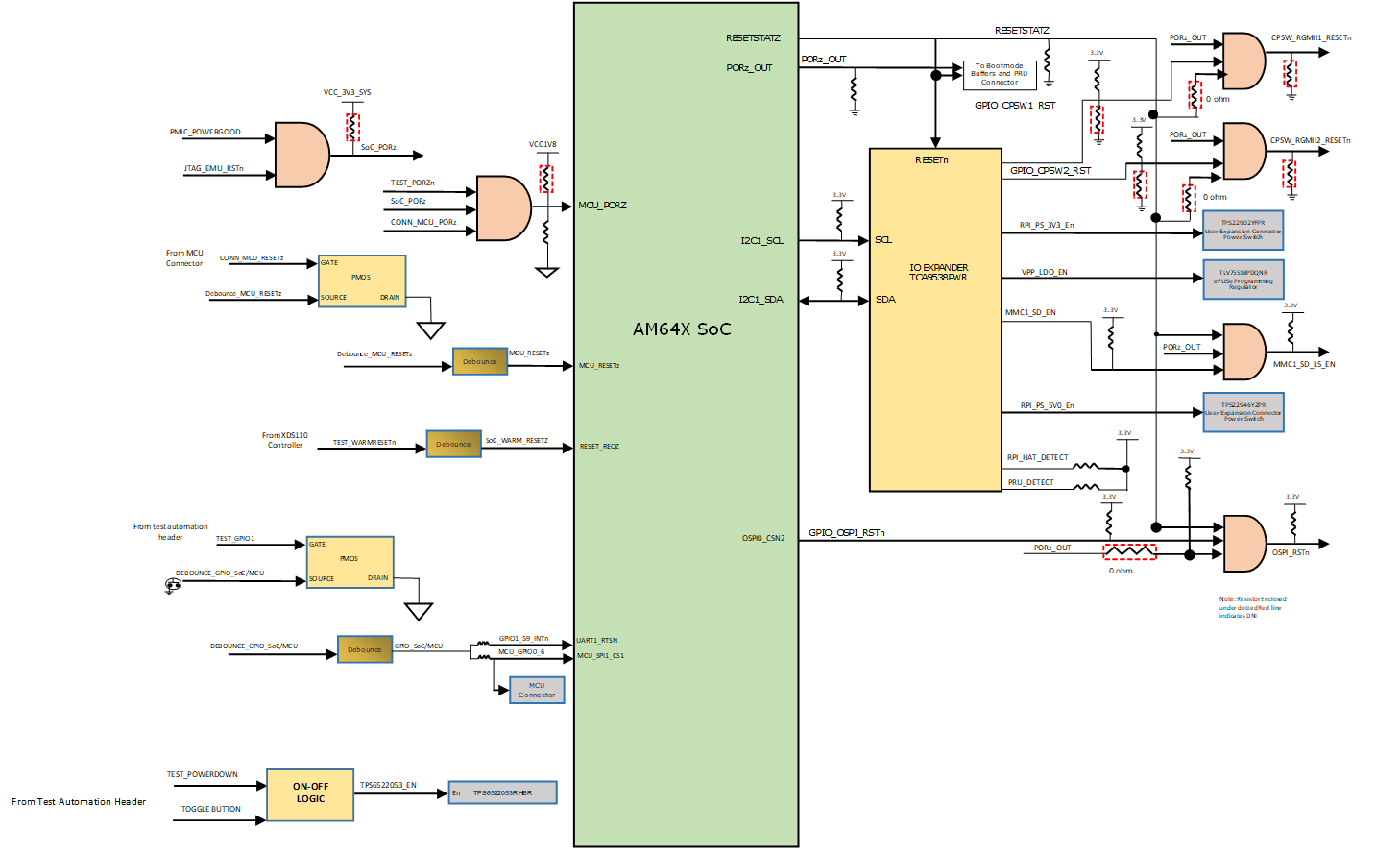
SoC_PORz signal is provided by ANDing the PGOOD signal of PMIC and JTAG emulator reset. MCU_PORz is provided by ANDing the CONN_MCU_PORz from MCU Connector, TEST_PORZn from Test Automation Connector and SoC_PORz.
MCU Domain warm reset (MCU_RESETz) and MCU Domain cold reset (MCU_PORz) of the SoC is achieved by CONN_MCU_RESETz and CONN_MCU_PORz respectively from the Safety Connector.
Upon Power on Reset, all peripheral devices connected to the main domain get reset by RESETSTATz along with a GPIO control as shown in Figure 4-7.
 Figure 4-7 Overall Reset
Architecture of the AM64x SK Event