SSZT796 february 2018 ESD122 , ESD2CAN24-Q1 , TPD1E01B04 , TPD1E01B04-Q1 , TPD1E05U06 , TPD1E0B04 , TPD1E10B06 , TPD1E10B09 , TPD4E02B04 , TPD4E05U06 , TPD4E1U06
In the third installment of this series, I explored the importance of the clamping voltage of an electrostatic discharge (ESD) protection diode.
Although the main goal of an ESD diode is to protect a system during an ESD event, it has another equally important purpose to fulfill during normal operation: do absolutely nothing. While “doing nothing” may seem like an easy task, the presence of an ESD diode adds parasitic capacitance to the system. During an ESD event, the diode will break down and steer the damaging current to ground. When the diode is conducting, it can be modeled as an offset voltage VBR (breakdown voltage) in series with a dynamic resistance (RDYN). During normal operation, the diode is reverse-biased while data (or power) transmits through the trace. As a result, the diode’s depletion region stores electric charge, effectively becoming a capacitor with capacitance value CL (Figure 1).
 Figure 1 During an ESD Event, the ESD
Diode Breaks Down at Voltage vBR And Has a Resistance of
RDYN (Left); During Normal Operation, Signals Pass to the System
and the ESD Diode Acts as a Capacitor with Capacitance Value CL
(Right)
Figure 1 During an ESD Event, the ESD
Diode Breaks Down at Voltage vBR And Has a Resistance of
RDYN (Left); During Normal Operation, Signals Pass to the System
and the ESD Diode Acts as a Capacitor with Capacitance Value CL
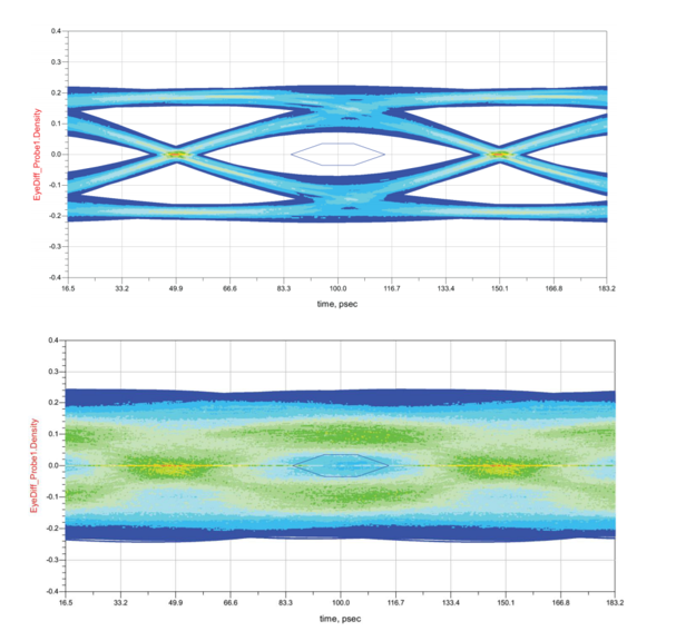
(Right)If you don’t properly account for CL, the diode will degrade the signal integrity of data passing through. For high-speed signals such as USB 3.0, USB 3.1 and High Definition Multimedia Interface (HDMI) 2.0, passing the eye-diagram mask test is required in order to achieve compliance with the interface standard. However, increased trace capacitance will increase signal rise and fall times and “shut” the eye. This could potentially push the entire system out of compliance (Figure 2).
 Figure 2 A Compliant USB 3.1 Gen 2 Eye
Diagram (Top); a Noncompliant USB 3.1 Gen 2 Eye Diagram Caused by High
Capacitance (Bottom)
Figure 2 A Compliant USB 3.1 Gen 2 Eye
Diagram (Top); a Noncompliant USB 3.1 Gen 2 Eye Diagram Caused by High
Capacitance (Bottom)Designers usually have a capacitance budget to ensure that the entire system stays within compliance – there is no blanket maximum ESD capacitance requirement applicable to every design. For example, if the traces of system A are shorter than that of system B, system A will have more leftover capacitance to allocate toward ESD protection. Therefore, the ESD diodes of system A can have a higher capacitance and still be compliant to the standard. While the exact maximum ESD capacitance value will vary from system to system, Table 1 lists general capacitance and device recommendations for several popular high-speed interfaces.
| Interface | ESD capacitance suggestion (CL) | TI recommended device |
|---|---|---|
| General-purpose input/output (GPIO) | <30pF | TPD1E10B06 |
| Push-button | <30pF | TPD1E10B06 |
| Audio | <10pF | TPD1E10B09 |
| USB 2.0 | <4pF | TPD1E05U06 |
| USB 3.2 Gen 1 | <0.5pF | TPD4E05U06 |
| USB 3.2 Gen 2 | <0.3pF | ESD122 |
| HDMI 1.4 | <0.7pF | TPD4E05U06 |
| HDMI 2.0 | <0.5pF | TPD4E02B04 |
| Ethernet | <4pF | TPD4E1U06 |
| Antenna | <0.2pF | TPD1E01B04 |
| CAN | <6pF | ESD2CAN24-Q1 |
| USB Type-C | <0.2pF | TPD1E0B04 |
| SerDes | <0.3pF | TPD1E01B04-Q1 |
In the fifth part of our article series, "ESD fundamentals, part 5: reverse working voltage, breakdown voltage and polarity configuration," we wrap up the ESD fundamentals series by covering the importance of reverse working voltage, breakdown voltage and ESD polarity configuration. Thanks for reading and feel free to leave a comment below!
Additional Resources
- View all articles in the ESD Fundamentals technical article series.
- Read these application reports: