TIDUEX5 October 2020
- Description
- Resources
- Applications
- Features
- 5
- 1System Description
- 2System Overview
-
3Hardware, Software, Testing Requirements, and
Test Results
- 3.1
Hardware Requirements
- 3.1.1 Getting Started
- 3.1.2 Testing and Results
- 3.1
Hardware Requirements
- 4Design and Documentation Support
2.3.2 INA302-Q1
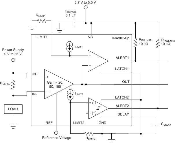
The INA302-Q1 and INA303-Q1 (INA30x-Q1) devices feature a high common-mode, bidirectional, current-sensing amplifier and two high-speed comparators to detect out-of-range current conditions. The INA302-Q1 comparators are configured to detect and respond to overcurrent conditions. The INA303-Q1 comparators are configured to respond to both overcurrent and under-current conditions in a windowed configuration. These devices feature an adjustable limit threshold range for each comparator set using an external limit-setting resistor. These current-shunt monitors can measure differential voltage signals on common-mode voltages that can vary from –0.1 V up to +36 V, independent of the supply. In addition, these devices will survive with common-mode voltages as high as 40 V.
The open-drain alert outputs can be configured to operate in either a transparent mode (output status follows the input state), or in a latched mode (alert output is cleared when the latch is reset). The alert response time for comparator 1 is under 1 µs, and the alert response for comparator 2 is set through an external capacitor ranging from 2 µs to 10 s.
These devices operate from a single 2.7-V to 5.5-V supply, drawing a maximum supply current of 950 µA. The devices are specified over the extended operating temperature range of –40°C to +125°C, and are available in a 14-pin TSSOP package.
 Figure 2-7 INA302-Q1 Block
Diagram