TIDUEX5 October 2020
- Description
- Resources
- Applications
- Features
- 5
- 1System Description
- 2System Overview
-
3Hardware, Software, Testing Requirements, and
Test Results
- 3.1
Hardware Requirements
- 3.1.1 Getting Started
- 3.1.2 Testing and Results
- 3.1
Hardware Requirements
- 4Design and Documentation Support
2.3.1 LM74810-Q1
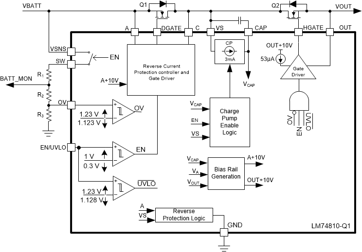
The LM74810-Q1 ideal diode controller drives and controls external back to back N-Channel MOSFETs to emulate an ideal diode rectifier with power path ON/OFF control and over voltage protection. The wide input supply of 3V to 65V allows protection and control of 12-V and 24-V automotive battery powered ECUs. The device can withstand and protect the loads from negative supply voltages down to –65 V. An integrated ideal diode controller (DGATE) drives the first MOSFET to replace a Schottky diode for reverse input protection and output voltage holdup. A strong charge pump of 3mA with 50mA peak GATE source current driver stage and short turn ON and turn OFF delay times ensures fast transient response ensuring robust and efficient MOSFET switching performance during automotive testing such as ISO16750 or LV124 where an ECU is subjected to input short interruptions and AC superimpose input signals up to 200KHz frequency. With a second MOSFET in the power path the device allows load disconnect (ON/OFF control) and over voltage protection using HGATE control. The device features an adjustable over voltage cut-off protection feature for load dump protection.
 Figure 2-6 LM74810-Q1 Block
Diagram