TIDUEX5 October 2020
- Description
- Resources
- Applications
- Features
- 5
- 1System Description
- 2System Overview
-
3Hardware, Software, Testing Requirements, and
Test Results
- 3.1
Hardware Requirements
- 3.1.1 Getting Started
- 3.1.2 Testing and Results
- 3.1
Hardware Requirements
- 4Design and Documentation Support
3.1.2.6.1 Cold Crank
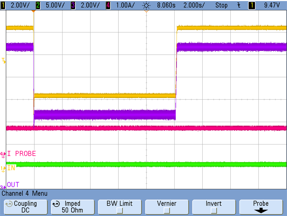
Cold crank testing is performed to ensure the design prevents reverse current during conditions where the input is lower than the output.
 Figure 3-11 Cold Crank Waveform
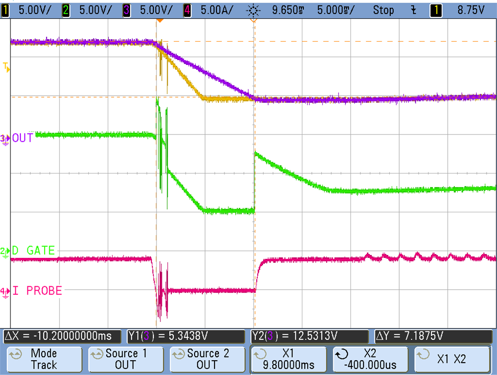
 Figure 3-12 Cold Crank Reverse Current
Testing
Figure 3-12 Cold Crank Reverse Current
TestingAs shown in Figure 3-11, the input voltage drops to be lower than the output voltage for a period of time before eventually moving back to normal voltage levels. In these cold crank events, LM74810 provides reverse current blocking through the use of the DGATE driven MOSFETs. As shown in Figure 3-12, the green trace which is the DGATE voltage, turns off when the input voltage drops to prevent reverse current to flow back to the battery. For the testing shown in Figure 3-12, the current load is set to a 4A load.