TIDUEY5 January 2021
3.3 Test Results
Cell Voltage Accuracy
When testing cell voltage accuracy, a resister divider should not be used to simulate battery cells. Since there will be some current flowing into cell input PINs when doing ADC measurement, the resister divider will cause further voltage drop and make the AFE readings lower than the actual value. It is good to use a real battery for testing. Another easy way is to utilize a DC source to stabilize the cell input voltage. This method was used in the design to test the cell voltage measurement accuracy. Figure 3-3 shows the cell voltage accuracy data without any further calibrations and under room temperature. All 16 channels of cell voltage error are below ±5 mV.
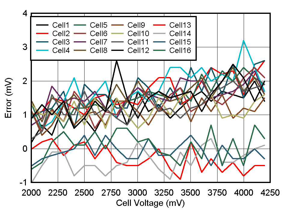 Figure 3-3 Cell Voltage
Accuracy.
 Pack Current Accuracy
This design uses two parallel 2-mΩ, 2-W, 50-PPM shunt resisters to measure pack current. Board offset was calibrated using the guidance of the Calibration section of the BQ76952 Evaluation Module User's Guide. Then Current Gain was calibrated with 5-A discharging current and also followed the guidance of the Calibration section of the BQ76952 Evaluation Module User's Guide. It is good to write the Board Offset and Current Gain values with OTP to BQ76952, otherwise the MCU has to store such data and write to BQ76952 every time it wakes up from shutdown mode. Figure 3-4 shows the pack current accuracy data under room temperature. The maximum current error is below ±10 mA when discharging current is below 2 A and ±0.5% when discharging current is above 2 A.
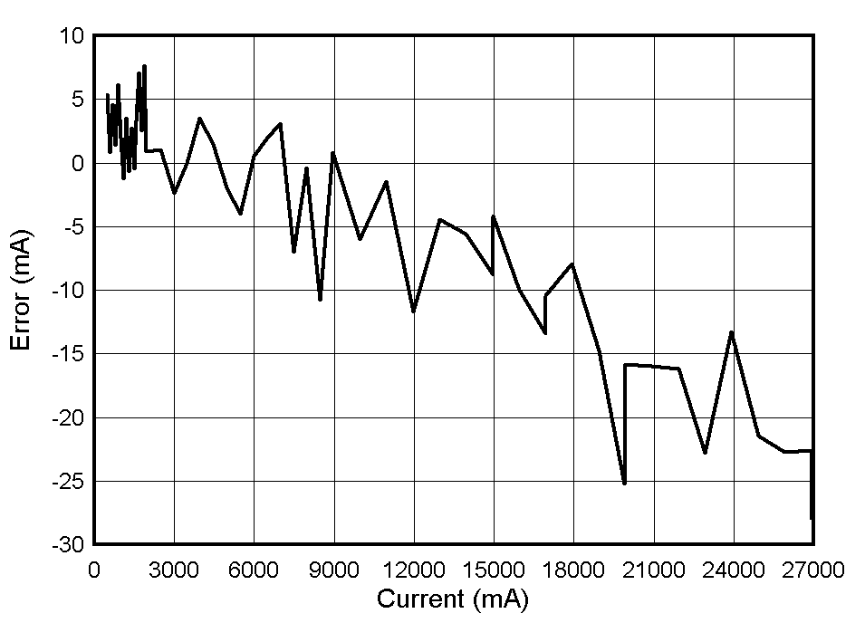 Figure 3-4 Pack Current Accuracy.
 Auxiliary Power and System Current Consumption
Thanks to the auxiliary power strategy, this design has very low current consumption, especially when in standby mode and ship mode. System-level current consumption contains 3 parts: (1) DC/DC current, (2) BQ76952 current (current into BQ76952 BAT PIN), (3) LDO current (current into BQ76952 REGIN PIN). This current could be measured from the voltage across (1) R115, (2) R61, and (3) R94. Table 3-5 shows the test results of current consumption.
| R115 (100 Ω) | R61 (100 Ω) | R94 (249 Ω) | Total Current (µA) | ||
|---|---|---|---|---|---|
| Standby Mode | Voltage (mV) | 0.66 | 2.02 | 11.45 | 72.8 |
| Current (µA) | 6.6 | 20.2 | 46 | ||
| Ship Mode | Voltage (mV) | 0.66 | 0 | 0 | 6.6 |
| Current (µA) | 6.6 | 0 | 0 | ||
Protection
The design integrates a full set of battery cell protections, including: cell overvoltage, cell undervoltage, two levels of overcurrent discharge, overcurrent charge, discharge short circuit, overtemperature and undertemperature protections. Furthermore, this design also monitors loss of system level faults, including: cell open wire, host watch dog, charge and discharge MOSFETs faults, MOSFETs overtemperature and so on. Some of the protections were tested in a TI lab.
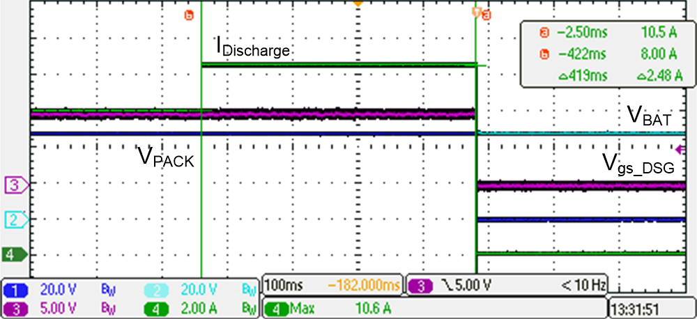 Figure 3-5 Level 1 Overcurrent
Discharge.
 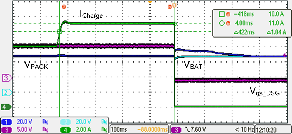 Figure 3-6 Overcurrent Charge.
 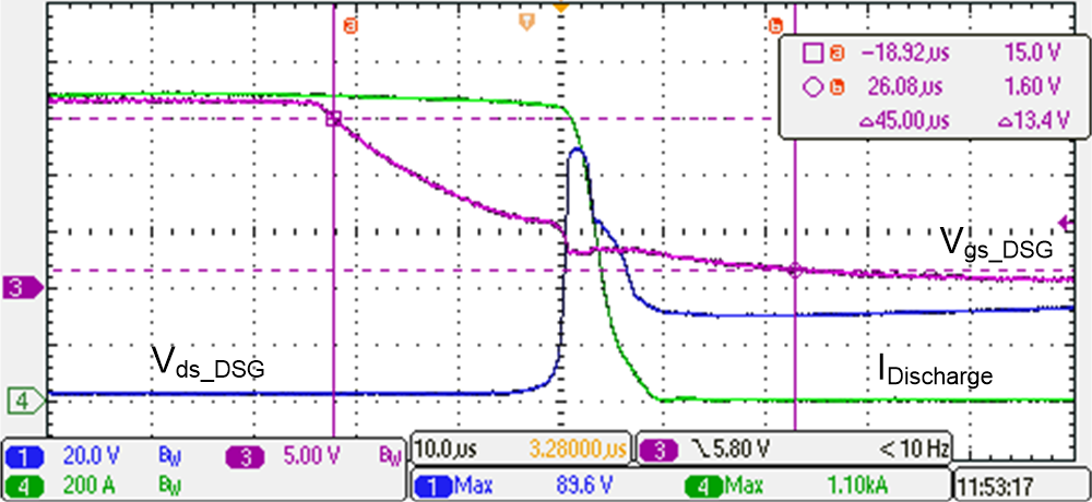 Figure 3-7 Discharge Short
Circuit.
 This design also gives the individual secondary protections to prevent the hazards from each cell overvoltage, each cell undervoltage and overtemperature. This helps to pass some safety regulations without further work. Secondary overvoltage and undervoltage protections were tested in a TI lab.
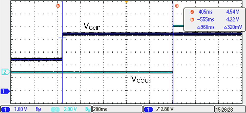 Figure 3-8 Secondary Overvoltage
Protection.
 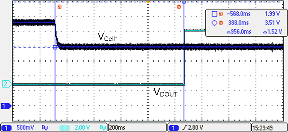 Figure 3-9 Secondary Undervoltage
Protection.
 Cell Balancing
The design board supports external cell balancing with 16 N-channel MOSFETs. The peak balancing current is 117 mA with 4-V cell voltage, 99 mA flows through external balancing resister and MOSFET, 18 mA flows through the BQ76952 device. This design only balances non-adjacent cells in use. The conditions that will trigger cell balancing are: minimum cell voltage is larger than 3500 mV, maximum cell voltage gap is larger than 40 mV, and cell temperature is between –20°C to 60°C. The external cell balancing performance is shown as Figure 3-10. Cell balancing duty is about 85%.
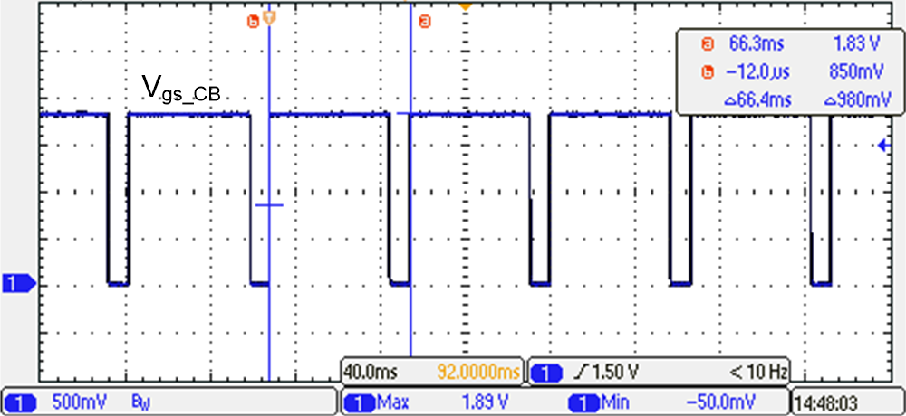 Figure 3-10 External Cell
Balancing.
 Working Modes Transition
This design has 3 working modes: normal mode, standby mode, and ship mode. When the pack is charging or discharging, it is in normal mode. Sleep mode is when no charging nor discharging, the pack is waiting for charger or load attachment. Shutdown mode is a very low current consumption mode which saves energy and helps to avoid battery over discharge when the pack or cell voltage is low. Different working mode transition are shown in Figure 3-11 to Figure 3-14.
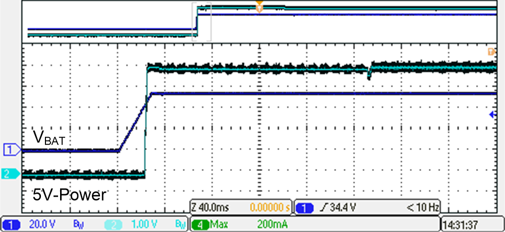 Figure 3-11 Shutdown Mode
to Normal Mode.
 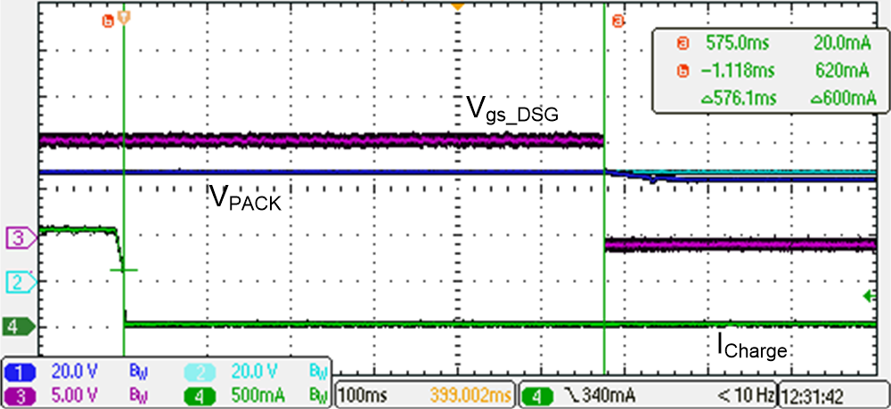 Figure 3-12 Normal Mode
(Charging) to Standby Mode.
 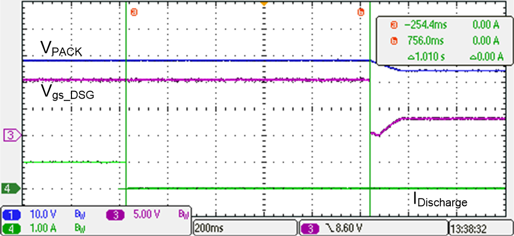 Figure 3-13 Normal Mode
(Discharging) to Standby Mode.
 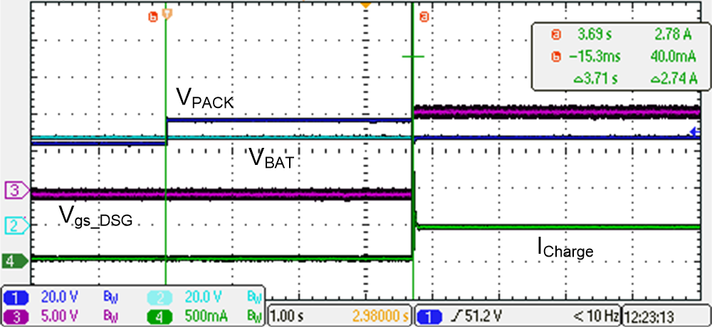 Figure 3-14 Standby Mode
to Normal Mode (Charge).
 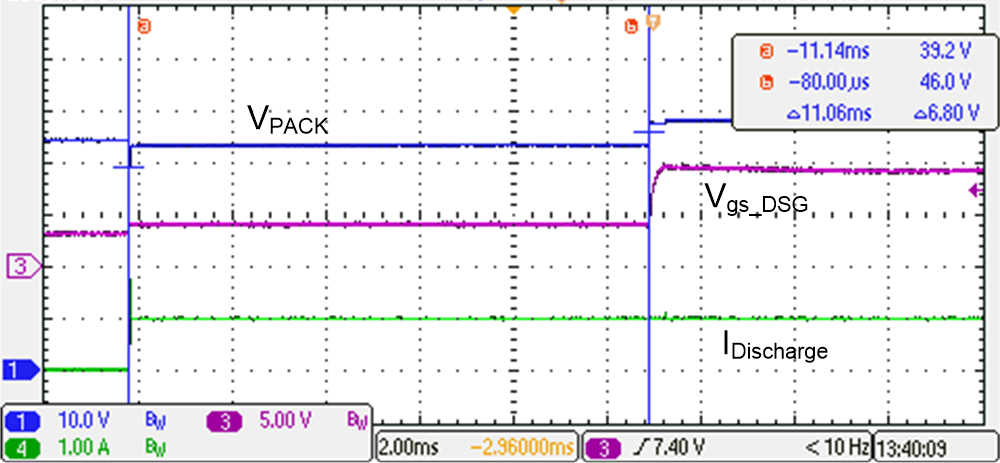 Figure 3-15 Standby Mode
to Normal Mode (Discharging).
 ESD Performance
The ESD performance of this design was tested in a TI lab per IEC 61000 - 4 - 2. Isolated DC source and resister divider are used to simulate battery pack. Only ESD contact discharge was tested and the test results are listed in Table 3-6.
Voltage | Applied Terminal | |
|---|---|---|
PACK+ | PACK– | |
2 kV | PASS | PASS |
–2 kV | PASS | PASS |
4 kV | PASS | PASS |
–4 kV | PASS | PASS |
8 kV | PASS | PASS |
–8 kV | PASS | PASS |