TIDUF09 December 2022
3.2 Test Setup
The TPS7A57EVM-081 reference design contains three parallel TPS7A57 LDO's with input, bias, NR/SS, and output capacitors installed, as well as PG and REF resistors installed. These components provide an implementation example, as illustrated by the white boxes in Figure 3-1. The prepopulated capacitors are sized to ensure the minimum capacitance requirements are maintained under all normal operating conditions. Optional pads are available to test the LDO with additional input, bias, and output capacitors beyond what is already installed on the EVM.
The TPS7A57EVM-081 is assembled for an output voltage of 0.75 V. For other voltage options, resistor R10 can be modified as necessary. See the Paralleling for Higher Output Current and Lower Noise section in the TPS7A57 data sheet for guidance on selecting R10 for alternate values of VOUT.
The TPS7A57 LDO can be enabled or disabled by using the J12 SMA connector:
- Tie the center pin of the SMA connector to a voltage source greater than 0.68 V and no greater than 6.5 V to enable the device
- Tie the center pin of the SMA connector to a voltage source less than 0.62 V to disable the device
Alternatively, by connecting an external function generator to TP1 (EN) and a nearby GND post (J17), the user can enable or disable the TPS7A57 LDO. If desired the user can populate the optional 3-pin headers J16, J10 and J3 to enable the parallel LDO's.
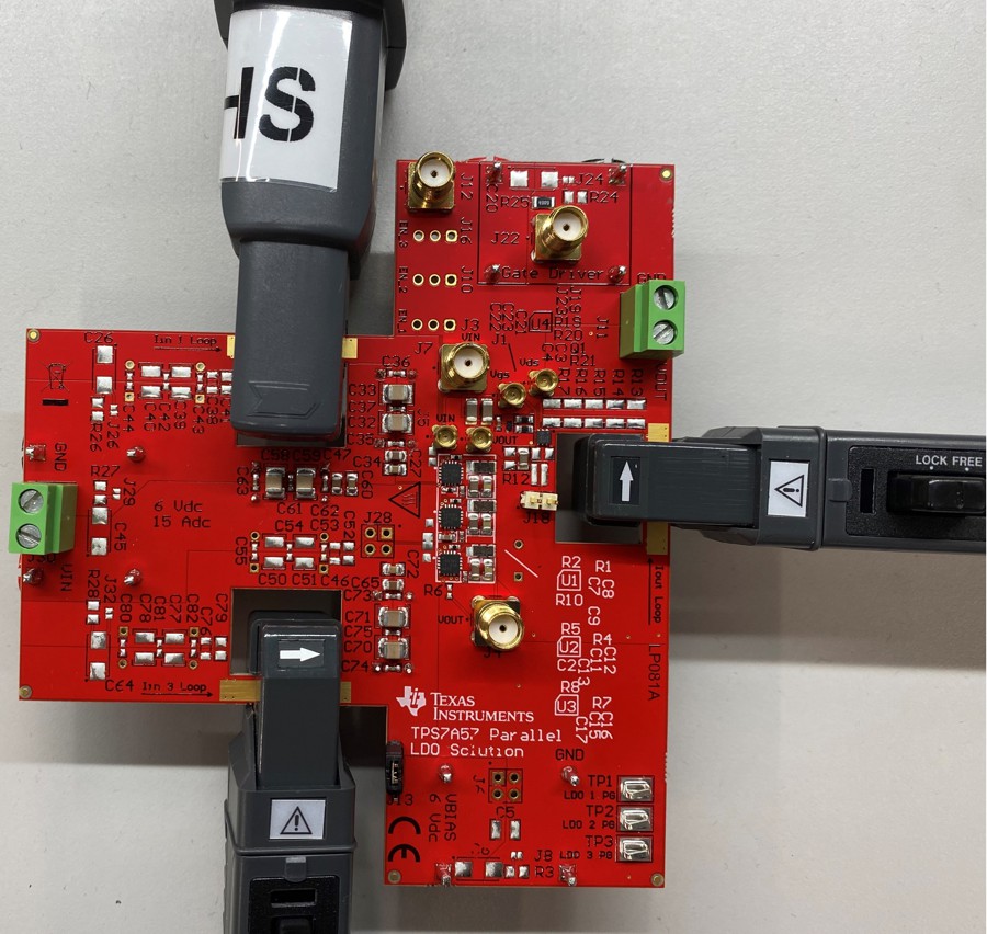
If desired, current probes can be inserted in the EVM as shown in Figure 3-1 to measure the input and output current. The slots were sized to fit most current probes, such as the LeCroy™ AP015 or CP031 current probes. The input current of two LDOs (the top and bottom LDOs) and the output current of all three LDOs can be measured directly using the current probes. To measure the current of the third (middle) LDO, subtract the top and bottom LDO current from the output current of all three LDOs:
 Figure 3-1 TPS7A57EVM-081 With Current
Probes Attached
Figure 3-1 TPS7A57EVM-081 With Current
Probes AttachedJ11 can be used to place a DC load that flows through the current sense path on the output of the LDO. In cases where very fast transient tests are performed, ringing can occur on VIN or VOUT as a result of the PCB parasitic inductance. Placing a strip of wire on the exposed copper in the current path can reduce this ringing. 10 AWG wire can be used as needed. If ringing persists, install damping networks by adding a series resistor and capacitor in parallel with VIN. Locations where damping can be installed include C6 and R3, C20 and R24, C26 and R26, C45 and R27, and C64 and R28.
Optional kelvin sense points are provided using the SMA connectors J7 (VIN) and J4 (VOUT) and MMCX connectors J5 (VIN) and J1 (VOUT).