TIDUF44 January   2024


  1.   1
  2.   Description
  3.   Resources
  4.   Features
  5.   Applications
  6.   6
  7. 1System Description
    1. 1.1 Key System Specifications
  8. 2System Overview
    1. 2.1 Block Diagram
    2. 2.2 Highlighted Products
      1. 2.2.1 BQ76907
      2. 2.2.2 BQ76905
      3. 2.2.3 BQ77207
      4. 2.2.4 MSPM0L1106
      5. 2.2.5 TCAN1042
      6. 2.2.6 TPSM365R6V5
      7. 2.2.7 TLV704
      8. 2.2.8 TMP61
  9. 3System Design Theory
    1. 3.1 Primary Protection Design
    2. 3.2 Secondary Protection
    3. 3.3 Other Circuit Design
  10. 4Hardware, Software, Testing Requirements, and Test Results
    1. 4.1 Hardware Requirements
    2. 4.2 Software Requirements
    3. 4.3 Test Setup
    4. 4.4 Test Results
      1. 4.4.1 Cell Voltage Accuracy
      2. 4.4.2 Pack Current Accuracy
      3. 4.4.3 Protection
      4. 4.4.4 Cell Balancing
      5. 4.4.5 Working Modes Transition
      6. 4.4.6 Thermal Performance
  11. 5Design and Documentation Support
    1. 5.1 Design Files
      1. 5.1.1 Schematics
      2. 5.1.2 BOM
    2. 5.2 Tools and Software
    3. 5.3 Documentation Support
    4. 5.4 Support Resources
    5. 5.5 Trademarks
  12. 6About the Author

Thermal Performance

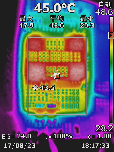
Figure 4-15 and Figure 4-16 show the thermal test in 18 VDC discharge current at about 15 A, the current waveform, and the thermal result.(Green:discharge Current, Blue:DSG V_gs)
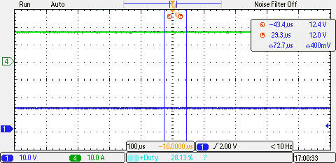
GUID-20230906-SS0I-WN2H-KXTQ-GLLLQK6ZTFQ3-low.pngFigure 4-15 Discharge in 15 A
GUID-20230906-SS0I-MTJM-KFJS-1WJXTJPTXP5Z-low.jpgFigure 4-16 Thermal Image in Discharge 15 A

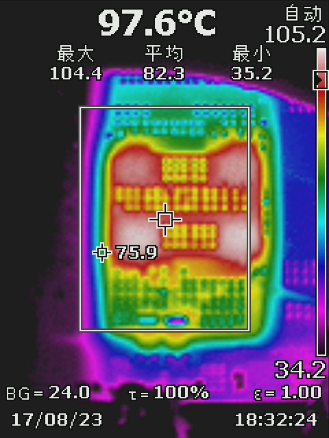
Figure 4-17 and Figure 4-18 show the thermal test in 18 VDC discharge current at about 30 A, the current waveform, and the thermal result.(Green:discharge Current, Blue:DSG V_gs, Cyan:Battery voltage)
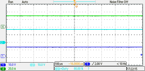
GUID-20230906-SS0I-4TFX-50LN-D0QRKLJXTLPD-low.pngFigure 4-17 Discharge in 30 A
GUID-20230906-SS0I-SJ9P-NB6K-RP0XCSJV0BN8-low.jpgFigure 4-18 Thermal Image in Discharge 30 A